





QR Code

Products
Contact Us


Fax
+86-579-87223657

E-mail

Address
Wangda Road, Ziyang Street, Wuyi County, Jinhua City, Zhejiang Province, China



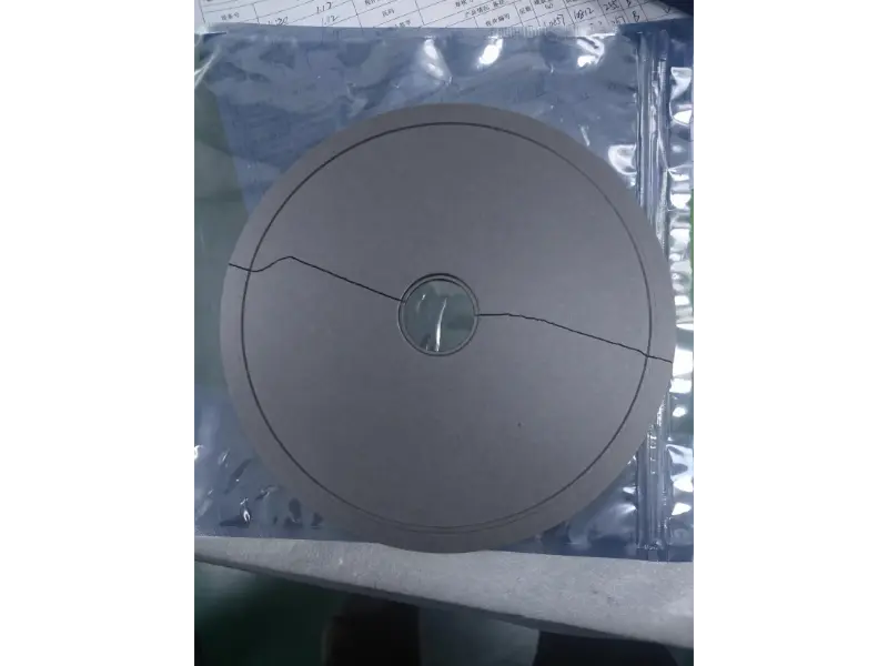
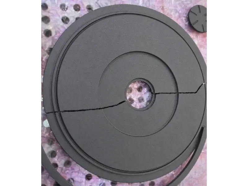
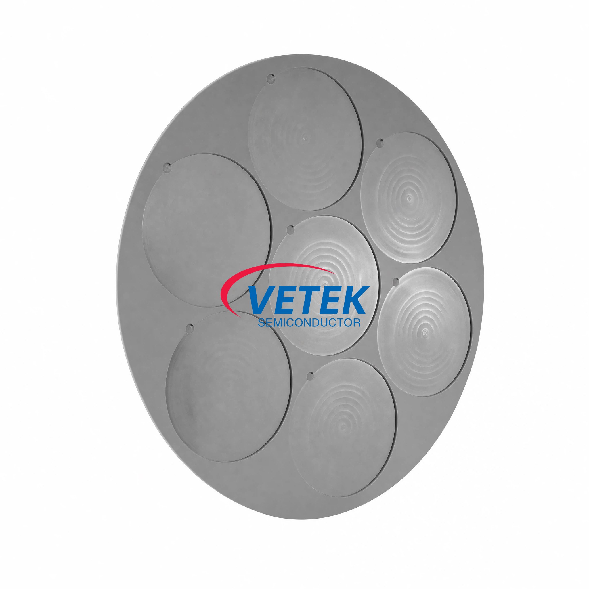
Figure 1,2: Radial Fracture Morphology of MOCVD CVD SiC-Coated Graphite Susceptor Originating from Central Step Thru-Hole
Core Conclusion: The design and quality of epitaxial wafer susceptors (wafer carriers) directly determine their service life, profoundly influencing epitaxy production cost allocation and equipment downtime. When selecting susceptors, epitaxial wafer manufacturers prioritize high-quality designs that tailor to actual process requirements, minimize replacement frequency, and extend service life—thereby achieving significant production cost reductions and steady improvements in epitaxial product quality.
By redesigning the stress-buffering zone at the central step and selecting graphite substrate materials with tailored Coefficient of Thermal Expansion (CTE), Vetek (www.veteksemicon.com) has completely resolved the industrial challenge of radial cracking originating from the central step thru-hole in MOCVD wafer carriers.
An overseas 3rd-generation semiconductor epitaxial chip manufacturer faced severe production bottlenecks due to immediate cracking and damage of large-size Chemical Vapor Deposition Silicon Carbide (CVD SiC) coated graphite susceptors during high-temperature MOCVD epitaxial growth. Our technical team pinpointed the root causes: severe stress concentration at the central step and thermal expansion mismatch of the graphite substrate. Through structural margin reconfiguration (expanding stress buffer zones, upgrading floating step positioning) and optimal graphite material selection, we successfully eliminated cracking hazards for the client.
Key Performance & Metric Improvements:
· Susceptor Cracking Rate: Reduced from >15% down to 0%
· Average Cycle Service Life: Increased by 300%+
· Unplanned Equipment Downtime: Decreased by 95%
The client is a leading automotive-grade compound semiconductor chip manufacturer operating multiple large-size, high-temperature MOCVD/MBE production lines focused on mass production of high-power and RF device epitaxial wafers. Reaction chamber operating temperatures reach 1000°C–1400°C year-round, undergoing high-frequency induction heating and severe rapid heating/cooling thermal cycles. As the core component directly holding the epitaxial wafers, large-sized CVD SiC-coated graphite susceptors must maintain extreme structural stability and thermal uniformity under high-temperature, high-stress environments.
When utilizing traditional susceptor designs, epitaxial manufacturers long suffered from severe economic and capacity pain points:
· Frequent Replacements & Extremely Short Lifespan: Conventional designs failed to account for thermal expansion differentials under extreme high temperatures. Susceptors cracked in under several dozen cycles, with some failing immediately upon installation (cracking rate >15%).
· Costly Downtime & Cleaning Expenses: Once a susceptor cracked or shattered inside the chamber, the entire batch of epitaxial wafers was scrapped, accompanied by severe particle contamination. Each incident required 12–24 hours of chamber cooling, disassembly, cleaning, re-evacuation, and pressure/temperature testing. Direct losses from unplanned downtime and consumables reached tens of thousands of USD per event.
· High Single-Wafer Production Cost: As high-value consumables, frequent replacements caused excessive susceptor cost allocation per wafer. Simultaneously, downtime reduced Overall Equipment Effectiveness (OEE) across the production line, significantly driving up fixed overhead costs.
Physical Failure Morphology: Fracture analysis indicates that crack initiation originates precisely at the inner step of the central thru-hole, extending radially outward across both sides of the susceptor body.
Root Cause Investigation (Stress Mechanism):
· Material Thermal Expansion Mismatch: Under high-temperature working conditions (1000°C and above), a significant thermal expansion coefficient (CTE) mismatch exists between the graphite substrate and the SiC protective coating. Because the thermal expansion coefficient of graphite is higher than that of the SiC coating, the graphite substrate undergoes greater thermal expansion deformation during heating than the surface SiC layer. This generates substantial interfacial thermal stress, ultimately inducing cracking and failure of the graphite substrate body.
· Structural Defect in Stress Relief Area: The original design lacked a necessary transition buffer zone at the central step, forming a classic mechanical stress concentration point. Once expansion tension exceeded the tensile strength threshold of the graphite substrate, micro-cracks instantly initiated at the sharp step corner and tore outward.
To address central step cracking, the Vetek R&D and Engineering Team formulated a comprehensive technical clarification plan based on high-temperature Coefficient of Thermal Expansion (CTE) optimization:
Optimization Dimension
Original Design / Traditional
Vetek Re-engineered Solution
Central Step Structure
Sharp stepped transition with no buffer zone; highly concentrated stress.
Added a stress buffer zone at the root of the step, effectively dispersing high-temperature thermal stress.
Substrate & Coating Process
Standard graphite substrate with inadequate thermal uniformity.
Selected graphite materials with CTE closely matched to that of CVD Silicon Carbide.
The re-engineered susceptors underwent rigorous thermal cycling and volume line verification on the client's production line, achieving remarkable performance improvements:
· Complete Elimination of Thermal Stress Cracking: Optimized susceptors operated continuously for over 500 thermal cycles, reducing cracking and damage rate directly from >15% to 0%.
· Massive Reduction in Downtime Losses: Unplanned downtime caused by carrier breakage decreased by 95%, dramatically boosting overall line OEE.
· Multiplied Service Life & Cost Reduction: Average susceptor service life increased by 300%+, resulting in a substantial drop in allocated susceptor cost per epitaxial wafer.
· High-Purity Raw Material Selection: Premium high-density isostatic graphite substrate (7N purity, ash content <5 ppm) is selected to ensure flawless CTE matching with the CVD SiC coating.
· Precision Machining: 5-axis CNC precision cutting (tolerances held within ±0.005 mm) is utilized, creating precise stress relief buffer zones at critical features such as the central step.
· CVD SiC Deposition: High-temperature CVD processes deposit a dense 80–100 μm β-SiC layer, providing superior thermal uniformity and corrosion protection.
· 100% CMM Full Inspection: High-precision Coordinate Measuring Machines (CMM) automatically scan and measure pocket arrays, central step dimensions, and overall planarity.
· Cleanroom Packaging & Delivery: Cleaned in Class 100 cleanrooms and double-packed in vacuumed nitrogen packaging, delivered with customized EVA shockproof cases.
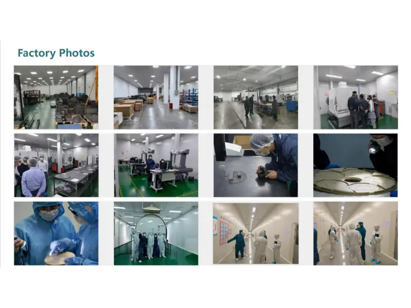
Figure 3: Vetek Semiconductor Advanced Precision Machining, Cleanroom & Quality Control Facilities
A: The primary cause is the lack of a stress-relief buffer zone at the central step, necessitating a structural redesign to distribute thermal stress.
A: No. SiC coatings primarily provide corrosion resistance, impurity prevention, and thermal conduction. If the structural design is flawed, the coating itself cannot withstand internal compressive and tensile stresses from the substrate. Only the combination of a 'rationally designed stress-buffering structure + high-quality CVD SiC coating' can thoroughly resolve cracking issues.
Although epitaxial wafer susceptors are auxiliary consumables, their structural design and manufacturing quality exert a pivotal impact on fab production efficiency and overall costs. Traditional designs often overlook material CTE matching and stress-concentration relief zones, leading to frequent susceptor failure, expensive downtime, and wafer scrap risks.
Through Vetek's structural optimization and refined thermal stress engineering, we not only helped the customer completely eradicate graphite susceptor cracking (reducing cracking rates to 0%), but also extended carrier service life by over 300%. This improvement significantly reduced replacement frequency, lowered per-wafer consumable allocation costs, and guaranteed the quality, stability, and continuity of wafer epitaxial growth—delivering substantial economic and capacity value.
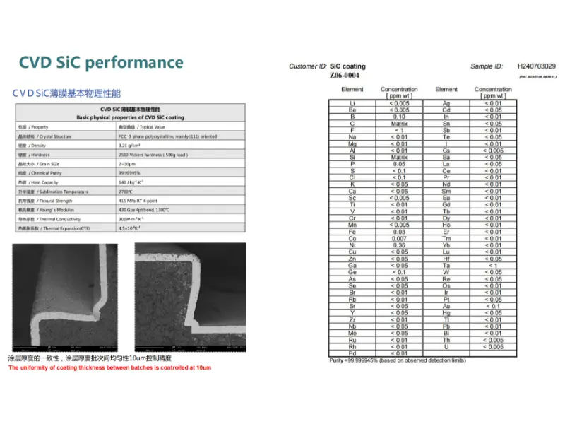
Figure 4: Key Physical Properties, SEM Thickness Uniformity, and Ultra-High Purity Analysis of CVD SiC Coating
Contact Us for Customized Thermal Stress Optimization Solutions
Are your MOCVD/MBE reaction chamber graphite carriers also facing high-temperature thermal stress cracking, SiC coating peeling, or short service life issues?
Vetek (www.veteksemicon.com) brings over 10 years of experience in semiconductor CVD SiC coating and high-purity graphite precision machining.
Submit your dimensional drawings or failed sample photos to receive a free thermal stress tolerance evaluation and trial testing service!

+86-579-87223657
Wangda Road, Ziyang Street, Wuyi County, Jinhua City, Zhejiang Province, China