
Products

Wafer

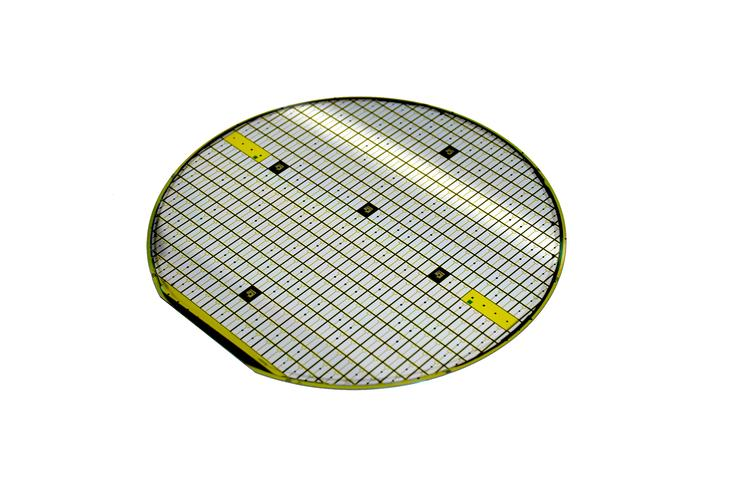
Wafer Substrate is a wafer made of semiconductor single crystal material. The substrate can directly enter the wafer manufacturing process to produce semiconductor devices, or it can be processed by epitaxial process to produce epitaxial wafers.

Wafer Substrate, as the basic supporting structure of semiconductor devices, directly affects the performance and stability of the devices. As the "foundation" for semiconductor device manufacturing, a series of manufacturing processes such as thin film growth and lithography need to be carried out on the substrate.
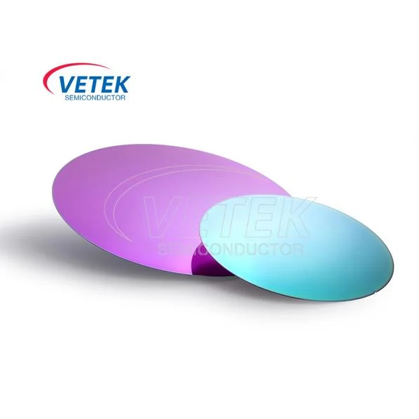
Summary of substrate types

  • Single crystal silicon wafer: currently the most common substrate material, widely used in the manufacture of integrated circuits (ICs), microprocessors, memories, MEMS devices, power devices, etc.;
  • SOI substrate: used for high-performance, low-power integrated circuits, such as high-frequency analog and digital circuits, RF devices and power management chips;
  • Silicon On Insulator Wafer Product Display

  • Compound semiconductor substrates: Gallium arsenide substrate (GaAs): microwave and millimeter wave communication devices, etc. Gallium nitride substrate (GaN): used for RF power amplifiers, HEMT, etc. Silicon carbide substrate (SiC): used for electric vehicles, power converters and other power devices Indium phosphide substrate (InP): used for lasers, photodetectors, etc.;
  • Sapphire substrate: used for LED manufacturing, RFIC (radio frequency integrated circuit), etc.;


Vetek Semiconductor is a professional SiC Substrate and SOI substrate supplier in China. Our 4H semi-insulating type SiC substrate and 4H Semi Insulating Type SiC Substrate are widely used in key components of semiconductor manufacturing equipment.

Vetek Semiconductor is committed to providing advanced and customizable Wafer Substrate products and technical solutions of various specifications for the semiconductor industry. We sincerely look forward to becoming your supplier in China .


Key Features

  • Professional supplier of SiC substrates (4H N-type & semi-insulating) and SOI substrates for power, RF and advanced IC applications.
  • Broad substrate portfolio covering silicon, compound semiconductors (SiC, GaN, GaAs, InP), sapphire and specialized wafers (PZT, SiN, dummy wafers).
  • High material quality and process consistency suitable for epitaxial growth, device fabrication and equipment process control.
  • Customizable specifications and technical solutions tailored to different semiconductor manufacturing requirements.
  • Reliable China-based supply with application engineering support for power devices, MEMS, LED, RF and thermal process tools.


Product Categories

  • SiC Substrates:4H N-type and semi-insulating SiC wafers for power devices and RF applications
  • SOI Substrates:Silicon-on-Insulator wafers for high-performance, low-power ICs and RF devices
  • Specialty / Process Wafers:CVD SiC coated dummy wafers, SiN substrates, PZT piezoelectric wafers on Si/SOI
  • Other compound / sapphire substrates:supporting LED, RF and optoelectronic applications (as referenced in overview)


Applications

To meet the diverse needs of semiconductor manufacturing, VeTek offers targeted Wafer Substrate products. The following table classifies them by major application areas:

Application Field Typical Products Application Description
Power Devices & EVs 4H-SiC substrates (N-type / semi-insulating) Silicon carbide substrates for power converters, electric vehicles and high-voltage power devices requiring high temperature and high efficiency performance.
RF / High-Frequency ICs SOI substrates, GaN / GaAs related substrates, semi-insulating SiC High-performance, low-power substrates for RF devices, power amplifiers, HEMTs and high-frequency analog/digital circuits.
MEMS & Sensors PZT piezoelectric wafers (PZT on Si/SOI), SiN substrates Piezoelectric and high-strength substrates for MEMS transducers, sensors, 5G, medical and wearable devices requiring electromechanical conversion.
Process Control & Testing CVD SiC coating Dummy wafer Dummy and test wafers for equipment qualification, process monitoring and contamination control in semiconductor manufacturing lines.
LED / Optoelectronics Sapphire substrates, compound semiconductor substrates (InP etc.) Substrates for LED manufacturing, lasers, photodetectors and RFIC applications requiring optical and high-frequency performance.
Advanced IC / Logic & Memory Single crystal silicon wafers, SOI substrates Mainstream and advanced substrates for integrated circuits, microprocessors, memories and power management chips.

For more detailed process matching solutions, please refer to the Silicon Carbide Epitaxy and Silicon Epitaxy related pages.


As a professional Wafer manufacturer and supplier in China, we have our own factory. Whether you need customized services to meet the specific needs of your region or want to buy advanced and durable Wafer made in China, you can leave us a message.
View as  
 
Aluminum Nitride (AlN) Wafers

Aluminum Nitride (AlN) Wafers

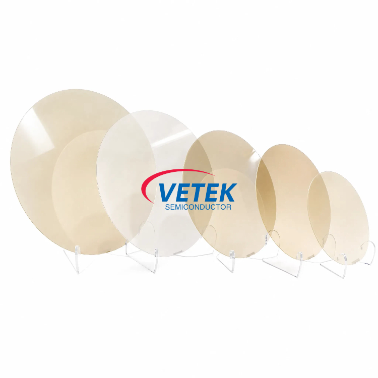
VeTek Semiconductor supplies high-quality Aluminum Nitride (AlN) single-crystal wafers and substrates for next-generation ultra-wide-bandgap semiconductor devices. With an ultra-wide bandgap of approximately 6.2 eV, outstanding thermal conductivity, exceptional electrical insulation, and excellent lattice and thermal-expansion match with GaN, AlN wafers are ideal for high-power RF devices, high-voltage power electronics, and deep-ultraviolet (DUV) optoelectronics.
PZT Piezoelectric Wafers (PZT on Si/SOI)

PZT Piezoelectric Wafers (PZT on Si/SOI)

As the demand for high-sensitivity and low-power MEMS transducers grows with the expansion of 5G communications, precision medical devices, and smart wearables, our PZT on Si/SOI wafers provide a critical material solution. Utilizing advanced thin-film deposition processes such as Sol-gel or sputtering, we achieve exceptional consistency and superior piezoelectric performance on silicon substrates. These wafers serve as the fundamental core for electromechanical energy conversion.
CVD SiC coating Dummy wafer

CVD SiC coating Dummy wafer

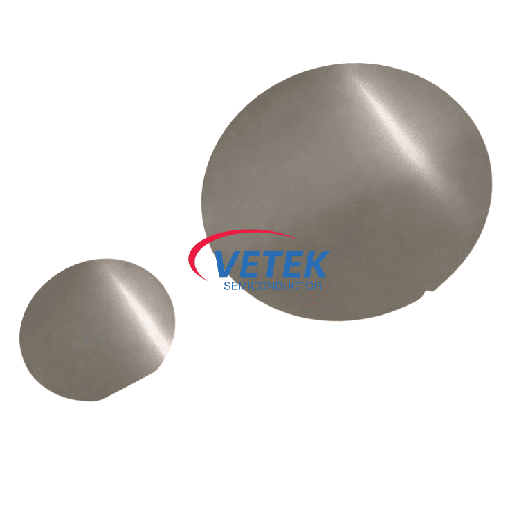
As a leading Chinese sic wafer manufacturers and suppliers, VeTek Semiconductor CVD SiC coating Dummy wafer is a specialized tool in semiconductor manufacturing, mainly used for the purpose of silicon wafer testing and wafer testing process. Your further inquiries are welcome.
SiN substrate

SiN substrate

VeTek Semiconductor is a leading manufacturer and supplier of SiN Substrate products in China. Our Silicon Nitride substrate has excellent thermal conductivity, excellent chemical stability and corrosion resistance, and excellent strength, making it a high-performance material for semiconductor applications. VeTekSemi SiN substrate ensures that you benefit from cutting-edge technology in the field of semiconductor processing, strict quality control, and welcomes your further consultation.
As a professional Wafer manufacturer and supplier in China, we have our own factory. Whether you need customized services to meet the specific needs of your region or want to buy advanced and durable Wafer made in China, you can leave us a message.
X
We use cookies to offer you a better browsing experience, analyze site traffic and personalize content. By using this site, you agree to our use of cookies. Privacy Policy
RejectAccept