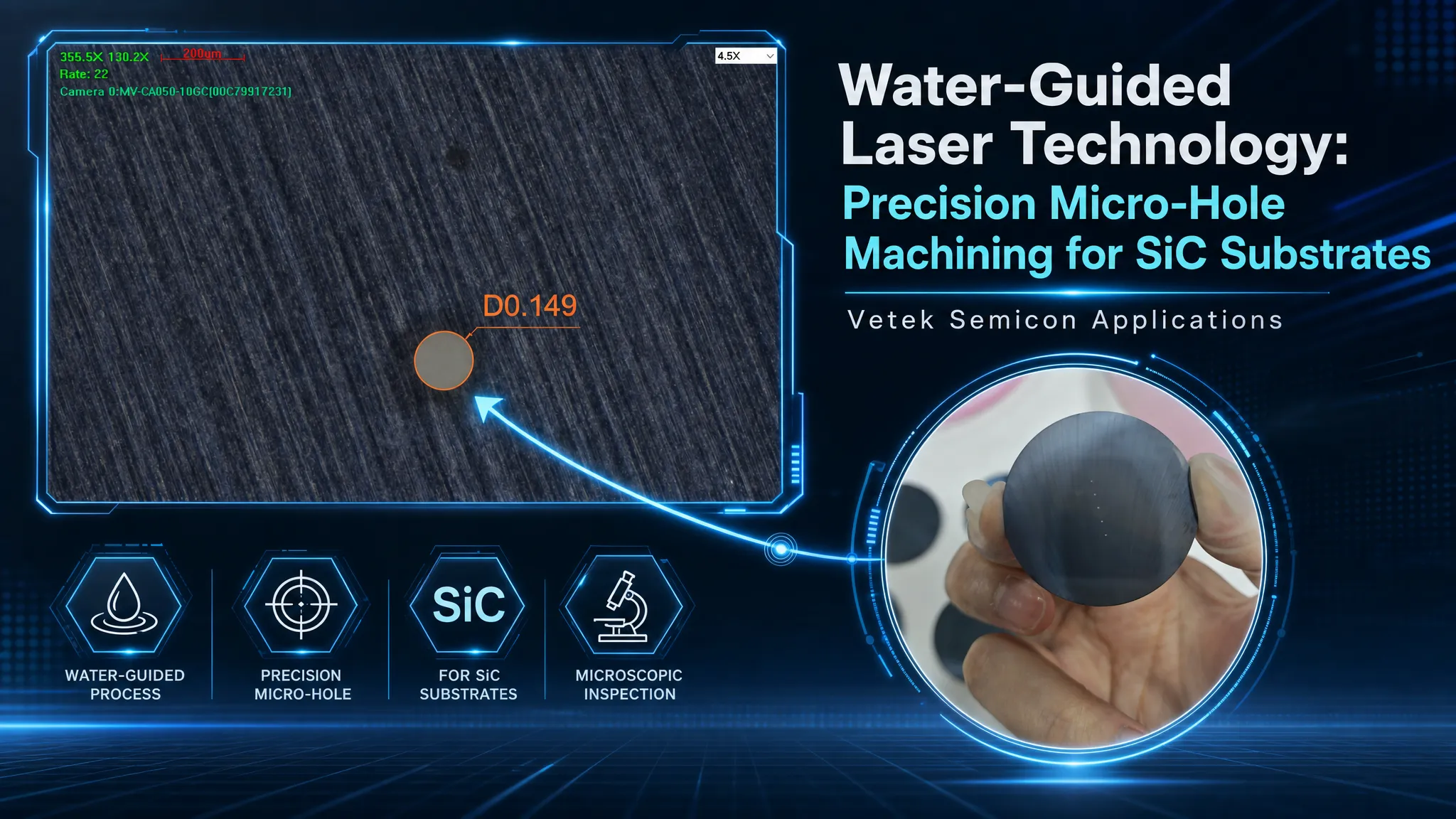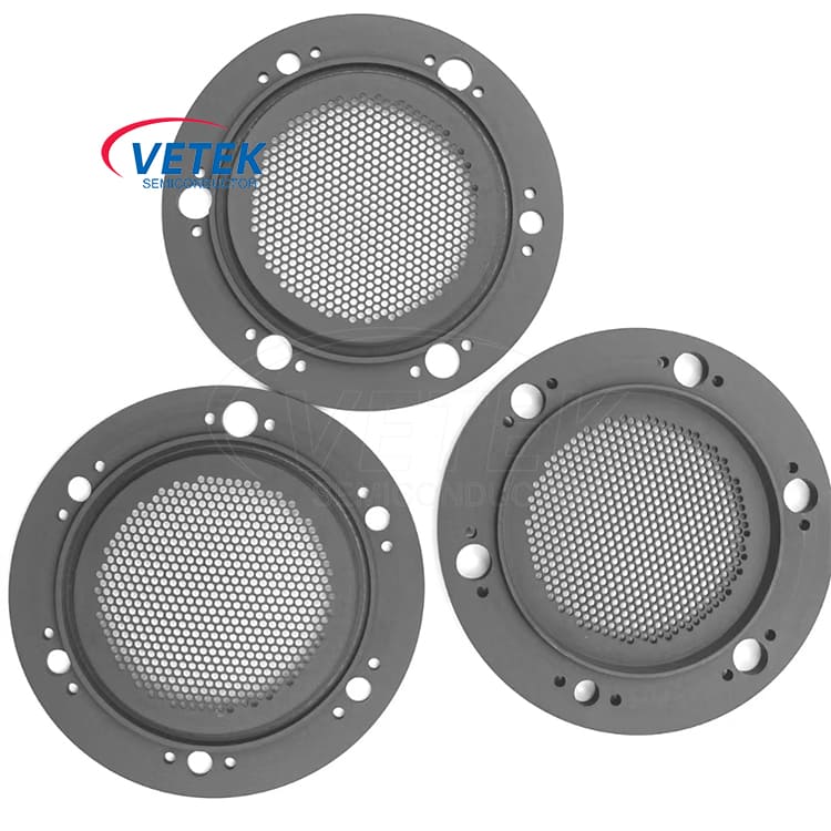

Discover how VeTek’s water-guided laser technology delivers uniform Φ0.15mm through-holes in 2mm SiC substrates with no taper, minimal HAZ and high yield for semiconductor applications.
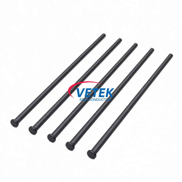
The most challenging technical issue for semiconductor equipment hollow lift pins is not the outer surface coating, but achieving stable and uniform CVD coating on the inner wall of the hollow structure. From inner-wall coating uniformity control to internal bore cleanliness assurance, every process step directly affects wafer yield. This article analyzes the core challenges of hollow lift pin inner-wall coating and the key technical pathways.
We use cookies to offer you a better browsing experience, analyze site traffic and personalize content. By using this site, you agree to our use of cookies. Privacy Policy