


QR Code

Products
Contact Us


Fax
+86-579-87223657

Email

Address
Wangda Road, Ziyang Street, Wuyi County, Jinhua City, Zhejiang Province, China


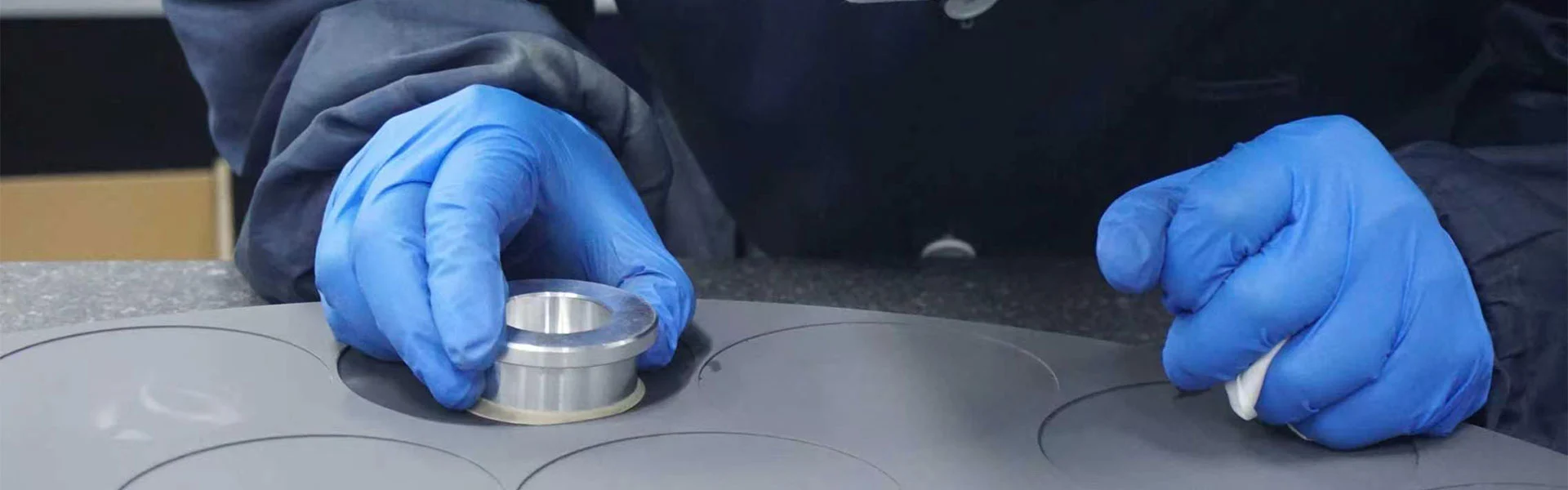
Selecting the matched substrate and coating combination is the key to preventing premature component failure, reducing particle contamination, and maximizing wafer yield. We provide tailored material and structural design solutions around the customer's specific process window (operating temperature, reactive gas chemistry, ramp rates).
| Coating | Typical Application Directions | Core Advantages |
|---|---|---|
| CVD SiC | Si/SiC epitaxy (Epi), MOCVD, partial plasma etching | High purity, good thermal stability, chemical corrosion resistance, high overall cost-performance |
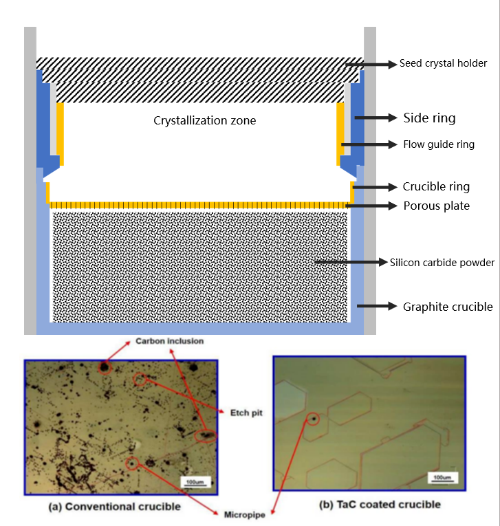
| CVD TaC | High-temperature SiC single-crystal growth (PVT), extreme high-temperature load-bearing components | Higher temperature rating (>1600 °C), strong corrosion resistance, excellent oxidation resistance |
A leading SiC epitaxy (Epi) manufacturer: The original component used a mismatched CVD TaC coating, resulting in excessive interfacial stress and frequent micro-cracks at high temperature. We re-ran thermodynamic simulations and switched to a CTE-matched specialty high-purity graphite substrate + buffer layer + CVD SiC coating solution. Result: average component lifetime increased from 200 hours to 850 hours; annual replacement frequency per tool dropped from 40 to 9 times; comprehensive equipment O&M cost savings exceeded RMB 650,000 per year.
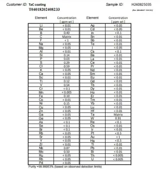
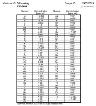
GDMS purity analysis report for TaC and SiC coatings
A: Look at your process temperature and gas-phase corrosion intensity. If the process temperature is below 1000 °C and mainly involves Cl₂/F₂-based etching or conventional epitaxy, choose CVD SiC for the best cost-performance; if the process temperature exceeds 1200 °C and involves strongly corrosive atmospheres (e.g., SiC PVT single-crystal growth), we recommend CVD TaC , which offers superior temperature and corrosion resistance. We can provide a free selection recommendation report based on your specific process parameters.
A: Yes! For reverse-engineering prototypes, MOQ is 1 piece . For conventional simple parts, from receipt of sample to delivery of the mapped part, the fastest lead time is approximately 10–15 working days ; for parts involving complex coating processes it is approximately 20–25 working days . Contact our engineers for expedited evaluation.
A: 90% of delamination cases are caused by mismatch between the coefficient of thermal expansion (CTE) of the graphite substrate and the coating, leading to fatigue peeling under rapid heating/cooling. Our solution: first precisely measure the CTE curve of your original part, then specially adjust substrate density and deposition temperature gradient so that the two CTEs are highly matched. Bond strength can be improved to more than 1.5 times the industry conventional level.
A: Every shipped product comes standard with a unique serial number + full CoA report . The report includes: critical dimension CMM inspection data, multi-point coating thickness distribution map, surface roughness (Ra) values, and material purity (GDMS) analysis conclusions.
Phone: +86-18069220752 (Tina); +86-15988690905 (Sera)
Email: anny@veteksemi.com
+86-579-87223657
Wangda Road, Ziyang Street, Wuyi County, Jinhua City, Zhejiang Province, China