




QR Code

Products
Contact Us


Fax
+86-579-87223657

Email

Address
Wangda Road, Ziyang Street, Wuyi County, Jinhua City, Zhejiang Province, China



Expanding Advanced SiC, TaC and PyC Coating Capabilities for the Next Generation Semiconductor Industry
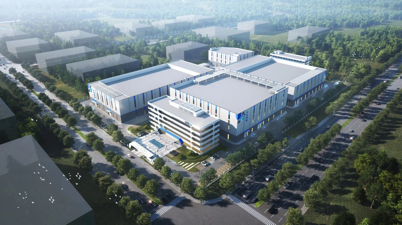
On 2025, VETEK officially celebrated the topping-out ceremony of its new semiconductor manufacturing base, marking a major milestone in the company’s expansion strategy for advanced semiconductor materials and coating technologies.
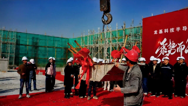
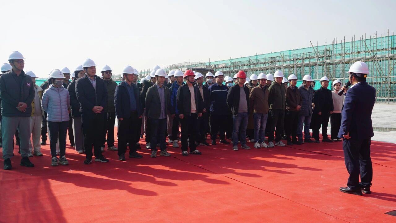
Government representatives, strategic partners, construction teams, and VETEK employees gathered together to witness this important moment and celebrate the rapid progress of the new facility.

As the final section of concrete was poured, the ceremony reached its climax amid applause and celebratory salutes — symbolizing not only the completion of a construction phase, but also the beginning of a new chapter for VETEK’s future development.
Accelerating Semiconductor Materials Manufacturing Capacity
The new production base is a key strategic project for VETEK in response to the rapidly growing global demand for semiconductor process materials and high-temperature coating solutions.
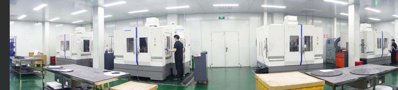
The facility will significantly enhance VETEK’s manufacturing and engineering capabilities in:
• CVD Silicon Carbide (SiC) Coating
• CVD Tantalum Carbide (TaC) Coating
• Pyrolytic Carbon (PyC) Coating
• Solid Silicon Carbide (Solid SiC)
• High Purity Graphite Components
• Semiconductor Thermal Field Materials
• Precision Machined Semiconductor Parts
Once fully operational, the new base will further strengthen VETEK’s integrated production capabilities covering:



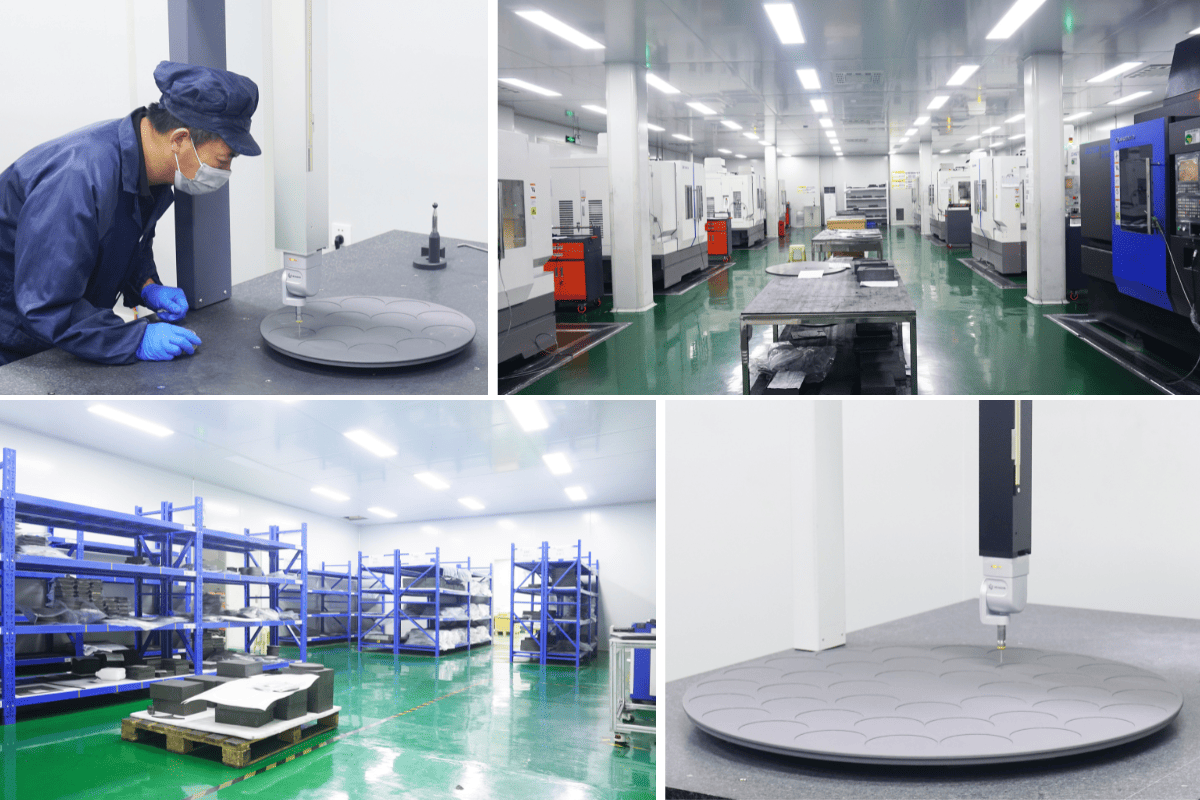
• Precision CNC machining
• Advanced CVD coating
• Semiconductor-grade cleaning
• Quality inspection and reliability testing
• Thermal field design and optimization
Supporting Key Semiconductor Processes
VETEK’s products are widely used in critical semiconductor manufacturing processes, including:
• SiC epitaxy
• Silicon epitaxy
• MOCVD processes
• Crystal growth systems
• RTP and etching applications
• Diffusion and oxidation processes
The company provides customized semiconductor components compatible with major industry platforms including:
• Aixtron
• Veeco
• AMEC
• LPE
• ASM
• Applied Materials (AMAT)
• Newflare
With the rapid growth of third-generation semiconductors, EV power devices, AI infrastructure, and advanced energy applications, demand for high-purity coating materials and thermal field components continues to increase worldwide.
Focus on Advanced Coating Technologies
VETEK continues to invest heavily in next-generation coating technologies designed for extreme semiconductor manufacturing environments.
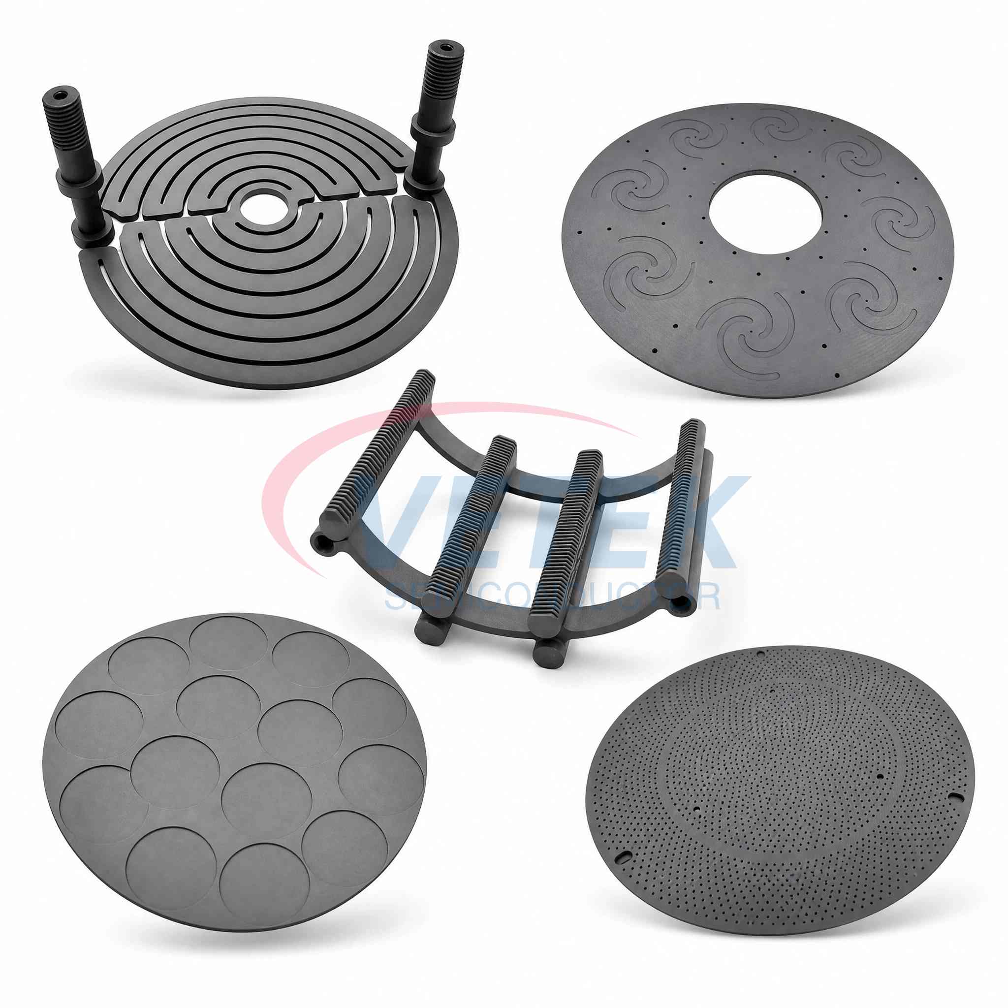
VETEK’s CVD SiC coated graphite products offer:
• Excellent thermal stability
• Superior chemical resistance
• Low particle contamination
• High purity performance
• Long service life under harsh process conditions
These products are widely used for:
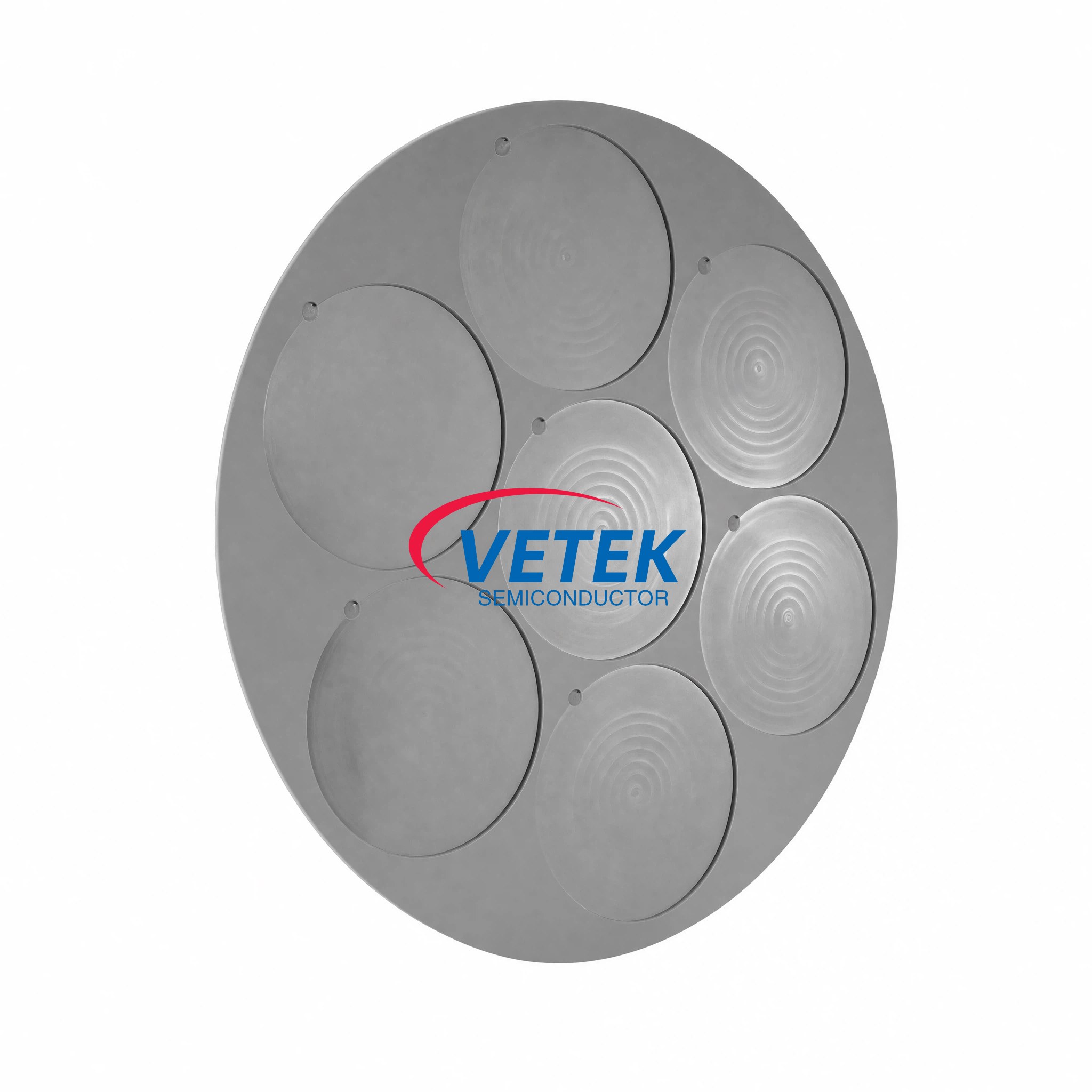
• Epitaxy susceptors
• Wafer carriers
• Barrel susceptors
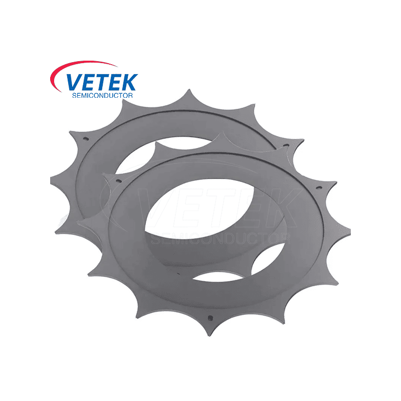
• Halfmoon parts
• Process components for SiC/GaN epitaxy
TaC Coating for Ultra-High Temperature Applications
As one of the company’s key development directions, VETEK’s TaC coating technology is engineered for ultra-high-temperature crystal growth environments exceeding 2000°C.
Compared with conventional SiC coatings, TaC coatings provide:
• Higher thermal stability
• Better anti-corrosion performance
• Superior resistance to graphite contamination
• Enhanced crystal growth environment stability
TaC coating products are increasingly important in:
• SiC single crystal growth
• PVT systems
• Advanced semiconductor thermal fields
Pyrolytic Carbon (PyC) Coating
VETEK also provides high-density PyC coating solutions featuring:
• Dense pore-free surfaces
• Excellent thermal shock resistance
• High vacuum compatibility
• Ultra-high purity performance
PyC coatings are widely used in:
• Semiconductor thermal processing
• Crystal growth furnaces
• High-temperature vacuum systems
Building the Future of Semiconductor Materials
During the ceremony, the project construction team emphasized its commitment to maintaining the highest engineering and quality standards to ensure smooth delivery of the facility.
The new manufacturing base represents the “VETEK Speed” in advanced semiconductor material industrialization — demonstrating the company’s determination to accelerate technology innovation and global supply capabilities.
Looking ahead, VETEK will continue to focus on:
• Advanced semiconductor coating technologies
• High-purity material innovation
• Thermal field engineering
• Semiconductor localization and supply chain reliability
The company remains committed to supporting the development of the global semiconductor industry through continuous technological innovation and high-quality manufacturing.
A New Milestone, A New Journey
The topping-out ceremony marks a new starting point for VETEK.
Carrying the vision of becoming a leading advanced semiconductor materials supplier, the new manufacturing base will further empower VETEK’s future growth and strengthen its position in the global semiconductor materials market.
As the semiconductor industry continues evolving toward higher temperatures, larger wafer sizes, and stricter purity requirements, VETEK is ready to move forward together with customers worldwide into the next generation of semiconductor manufacturing.
+86-579-87223657
Wangda Road, Ziyang Street, Wuyi County, Jinhua City, Zhejiang Province, China