
QR Code

Products
Contact Us


Fax
+86-579-87223657

Email

Address
Wangda Road, Ziyang Street, Wuyi County, Jinhua City, Zhejiang Province, China


In semiconductor manufacturing, surface treatment technology plays a crucial role in enhancing the durability, performance, and reliability of components by modifying their surface properties through advanced coating and deposition methods.
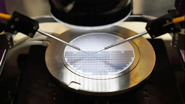
Physical Vapor Deposition PVD is a vacuum-based coating process that deposits thin films onto substrates through vaporization of solid materials. It enhances surface hardness, thermal resistance, and conductivity, making it essential for semiconductor tools and precision components.
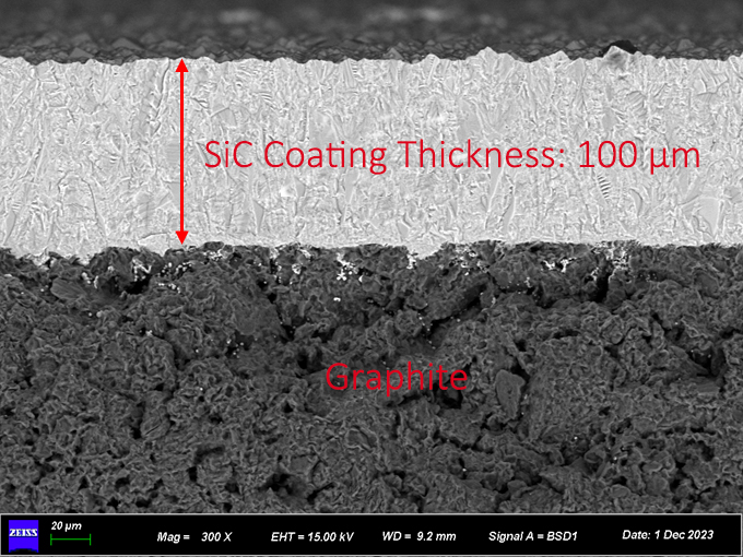
This technique involves high-temperature spraying of fine powders onto surfaces to create dense, protective coatings. It significantly boosts resistance to heat, wear, and corrosion in critical semiconductor components exposed to harsh environments.
MAX Phase nanopowders are layered ceramics with metallic properties, offering high strength, conductivity, and thermal shock resistance. They are ideal for protective coatings and emerging semiconductor applications requiring high-temperature stability.
To meet the diverse needs of semiconductor and precision manufacturing, VeTek offers targeted Surface Treatment Technology solutions. The following table classifies them by major technology and application areas:
| Technology / Field | Typical Products / Solutions | Application Description |
| Physical Vapor Deposition (PVD) | PVD thin-film coatings for tools and precision components | Vacuum-based deposition of thin films to enhance surface hardness, thermal resistance and conductivity for semiconductor tools and high-precision parts. |
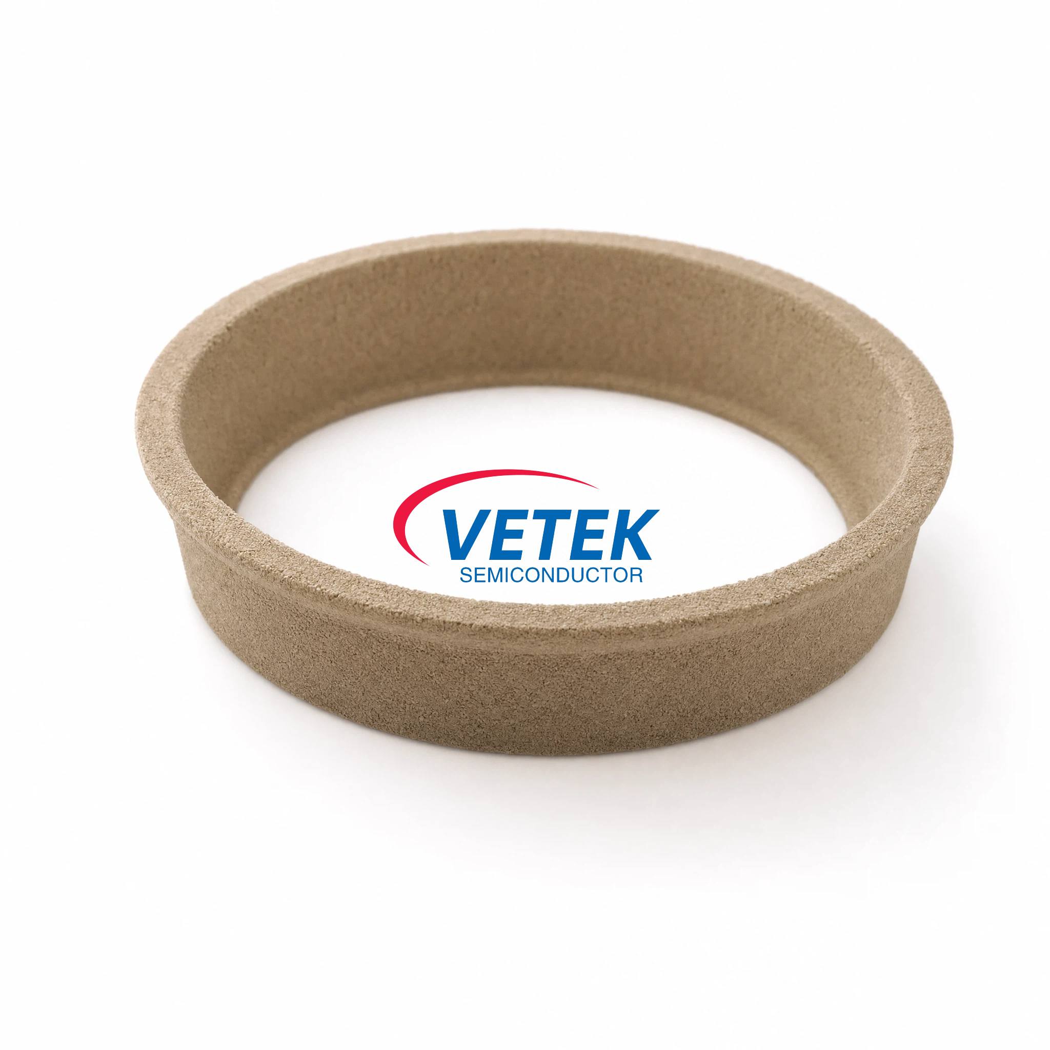
| Semiconductor Thermal Spraying | Thermal spray coatings, MLCC sintering crucible coatings | High-temperature spraying of powders to form dense protective coatings with heat, wear and corrosion resistance; widely used for semiconductor components and MLCC material sintering crucibles. |
| MAX Phase Materials | MAX Phase nanopowder | Layered ceramics with metallic properties for protective coatings and emerging semiconductor applications requiring high strength, conductivity and thermal shock resistance. |
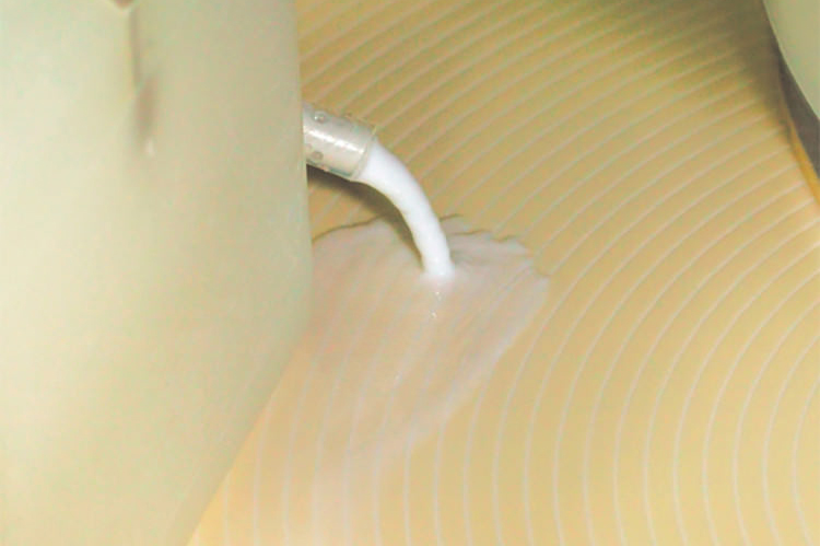
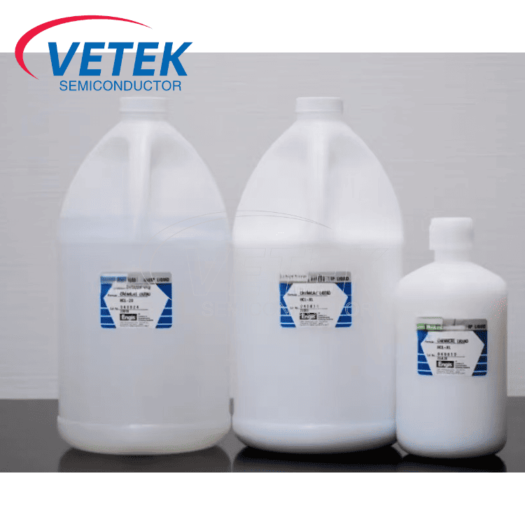
| CMP / Planarization | CMP Polishing Slurry | Chemical-mechanical polishing materials for nano-level surface flatness and quality in semiconductor manufacturing and precision material processing. |
| Component Protection & Lifetime | PVD and thermal spray protective coatings | Surface modification of critical semiconductor equipment parts to improve durability, reduce wear and extend service life in harsh process environments. |
For more related coating and materials solutions, please refer to the Tantalum Carbide Coating and Silicon Carbide Coating pages.
As a professional Surface Treatment Technology manufacturer and supplier in China, we have our own factory. Whether you need customized services to meet the specific needs of your region or want to buy advanced and durable Surface Treatment Technology made in China, you can leave us a message.


+86-579-87223657
Wangda Road, Ziyang Street, Wuyi County, Jinhua City, Zhejiang Province, China