

QR Code

Products
Contact Us


Fax
+86-579-87223657

Email

Address
Wangda Road, Ziyang Street, Wuyi County, Jinhua City, Zhejiang Province, China


VeTek Semiconductor's Technical services cover the purification and mapping of various semiconductor materials, aiming to provide customers with high quality semiconductor materials for a variety of applications. We have advanced purification technology and equipment to effectively remove impurities, thereby increasing the purity of semiconductor materials. Our purification process is carefully designed to include multiple steps and strict quality control to ensure the excellent purity and stability of the materials provided.
At the same time, we are committed to providing our customers with accurate and reliable mapping services. We have advanced test equipment and instruments, and rely on an experienced professional team, can conduct comprehensive measurement and analysis of the characteristics of semiconductor materials. Our mapping work includes tests of electrical properties, composition, purity, physical properties, etc., as well as in-depth studies of material structure and composition. Through mapping, we can obtain detailed data and information to provide customers with accurate assessment of material characteristics and relevant recommendations.
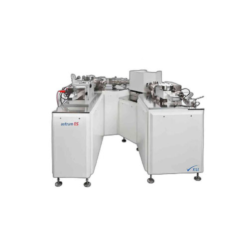 GDMS
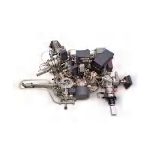 D-SIMS
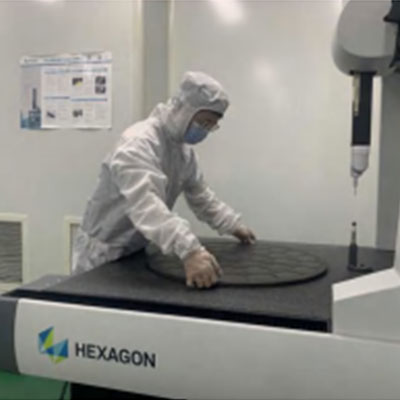 Coordinate measuring machine
VeTek Semiconductor has leading machining capabilities and experience for graphite, silicon carbide and other semiconductor products, which can meet customers' high precision and high purity.
High quality and other processing requirements. The tools we use, the cutting process and the choice of materials are also carefully optimized to achieve micrometer size control and control of the product
High surface quality. We pay attention to quality control and process optimization in the processing process, and carry out real-time monitoring and control of key parameters in the processing process to ensure the quality of products
Consistency and stability. We also implement a strict quality management system to ensure that products are processed in accordance with customer requirements and industry standards, and carry out comprehensive quality inspection.
We will continuously invest in equipment improvement and technological innovation to meet the growing needs of our customers and provide them with superior solutions and support.
In terms ofthemmal field design and transformation, our company can complete the design and batch supplyto Czochra single crystal, casting polycrystal, gallilum arsenide, zinc selenide, sapphire, silicon carbide and otherdiferent industry equipment. At the same time, for the mechanical thermal calculation ofvarious structures, components and atmospheres under different high temperature environments, we also have professionalmodeling and simulation computing capabilities, which can provide customers with professional designoptimization programs and suggestions.
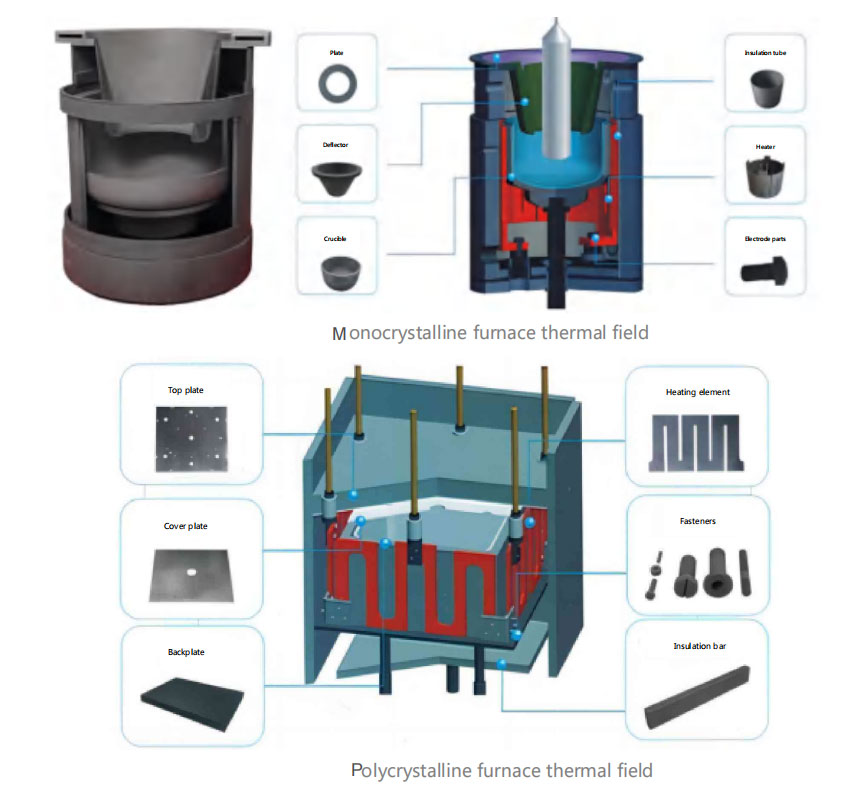
To meet the diverse needs of semiconductor materials and equipment customers, VeTek offers targeted Technical Services. The following table classifies them by major service areas:
| Service Area | Typical Services / Products | Application Description |
| Material Purification & Mapping | Purification processes; electrical / composition / purity / structure testing and analysis | Remove impurities and fully characterize semiconductor materials to ensure high purity, stability and accurate property assessment for various applications. |
| Precision Machining | Machining of graphite, silicon carbide and other semiconductor products | High-precision, high-purity machining with micrometer-level control and high surface quality for graphite and SiC components used in semiconductor equipment. |
| Thermal Field Design & Modification | Thermal field design and batch supply; thermal simulation and optimization | Design and supply of thermal fields for Czochralski, casting, GaAs, ZnSe, sapphire, SiC and other systems; mechanical-thermal calculation and design optimization under high-temperature conditions. |
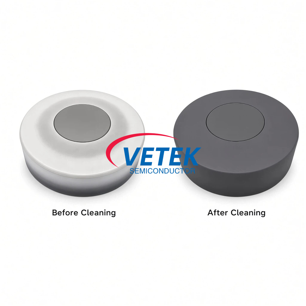
| Parts Cleaning (CVD SiC) | CVD SiC Coating Graphite Parts Cleaning Service | Specialized cleaning for Aixtron/Veeco MOCVD susceptors and graphite parts in GaN/AlN/AlGaN epi; removes memory effect, protects CVD SiC coating (zero thickness loss, zero metal residue). |
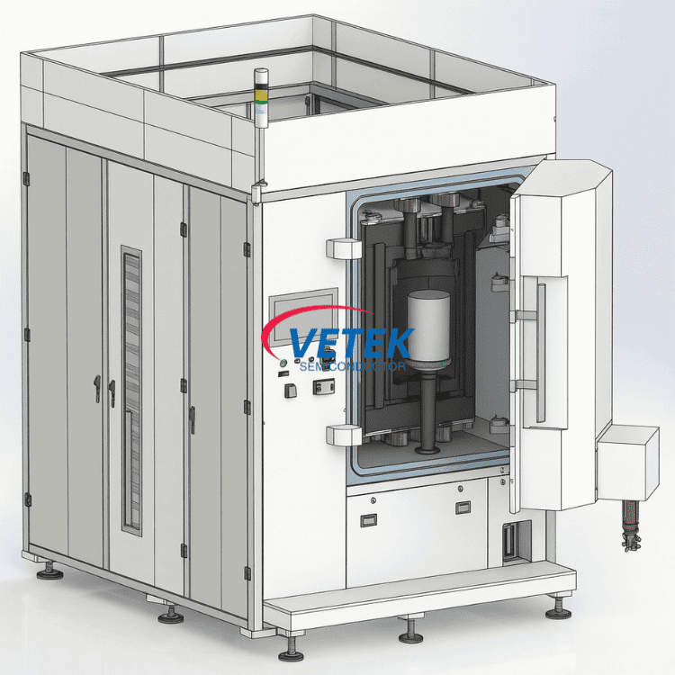
| Crystal Growth Equipment | Large sized resistance heating SiC crystal growth furnace | PVT-based resistance heating furnaces for stable 6–12 inch SiC crystal growth; precise control of temperature, pressure and power to reduce defects and support industrial production. |
For related materials and process solutions, please refer to the Silicon Carbide Coating, Special Graphite and Silicon Carbide Epitaxy pages
As a professional Technical Service manufacturer and supplier in China, we have our own factory. Whether you need customized services to meet the specific needs of your region or want to buy advanced and durable Technical Service made in China, you can leave us a message.
+86-579-87223657
Wangda Road, Ziyang Street, Wuyi County, Jinhua City, Zhejiang Province, China