






QR Code

Products
Contact Us


Fax
+86-579-87223657

E-mail

Address
Wangda Road, Ziyang Street, Wuyi County, Jinhua City, Zhejiang Province, China



In 2013, the industry asked whether silicon carbide could be commercialized at all. Ten years later, SiC powers EVs and renewable energy — and the real competition has shifted to materials, equipment, and manufacturing yield. In a decade, SiC wafers grew from 4-inch to 8-inch as epitaxy equipment advanced in step. Beyond the wafer itself, CVD SiC coatings, Solid CVD SiC, and TaC coatings now keep high-temperature, corrosion-resistant equipment running reliably. VETEK Semiconductor supplies all three material solutions for scaled SiC manufacturing.
SiC has moved from a promising lab material in 2013 to a mainstream technology underpinning EVs, power electronics, and energy conversion today — and the industry's focus has shifted from proving the technology to mastering manufacturing at scale.
The table below summarizes how the SiC industry's priorities changed over the past decade.
2013 vs. Today: How the SiC Industry's Focus Has Shifted
|
Dimension |
2013 |
Today |
|
Industry stage |
Moving from R&D to early commercialization |
Mainstream deployment across EV, power electronics, energy |
|
Mainstream wafer size |
4-inch transitioning to 6-inch (150mm) |
6-inch mainstream; 8-inch (200mm) qualification and ramp-up underway |
|
Central question |
Can SiC be commercialized? |
How to manufacture SiC with higher efficiency, fewer defects, and more consistency? |
|
Key focus areas |
Achieving 6-inch epitaxy, basic uniformity |
Yield improvement, defect reduction, batch stability, equipment uptime |
|
Materials attention |
Primarily wafers and devices |
Wafers, devices, and equipment components (coatings, hot-zone parts) |
Epitaxy equipment has always been the technical bottleneck for SiC commercialization — the industry's progress can be tracked directly through the evolution of epitaxy reactors, from early 6-inch platforms to today's automated 150mm/200mm systems.
In 2013, SiC commercialization was accelerating, and equipment makers were competing primarily around 6-inch (150mm) SiC epitaxy capability. Semiconductor Today reported on several representative systems at the time:
Representative SiC Epitaxy Equipment, 2013
|
Equipment Maker |
Model |
Technical Highlights |
|
Aixtron |
AIX G5 WW Planetary Reactor |
Supported 6×150mm or 10×100mm substrates, built for SiC epitaxy volume production |
|
LPE |
ACiS M8 / M10 |
Hot-wall CVD architecture, supporting multi-wafer SiC epitaxy production |
|
Tokyo Electron (TEL) |
Probus CVD System |
Supported up to 6-inch SiC epitaxy, configurable with dual reaction chambers |
These early systems were designed to solve four problems: achieving 6-inch SiC epitaxy, improving epitaxial layer uniformity, lowering defect density, and meeting the needs of early power-device commercialization.
As EV adoption, EV charging infrastructure, solar-plus-storage systems, and industrial power markets expanded rapidly, demand for SiC devices grew accordingly — and epitaxy equipment evolved from small-batch R&D platforms into next-generation systems built for large-scale manufacturing. Today's representative platforms include:
|
Equipment Maker |
Current Representative System |
Technical Highlights |
|
Aixtron |
G10-SiC |
Built for 150mm/200mm SiC epitaxy volume production, with higher capacity and automation |
|
LPE |
PE1O6 / PE1O8 Series |
Built for large-diameter SiC epitaxy using advanced hot-wall CVD technology |
|
Tokyo Electron (TEL) |
TEL SiC Epi Reactor |
Built for high-reliability SiC power device manufacturing, emphasizing automation and production stability |
|
NuFlare Technology |
SiC Epitaxy System |
Built for advanced SiC epitaxy manufacturing requirements |
|
Applied Materials |
SiC epitaxy platform |
Expanding into third-generation semiconductor manufacturing equipment |
Every step up in SiC wafer diameter — from 4-inch to 6-inch, and now toward 8-inch — exists to raise output per wafer and lower manufacturing cost, and the industry is now in the middle of the 6-inch-to-8-inch transition.
In 2013, the SiC industry was pushing to move from 4-inch to 6-inch wafers. Companies including Cree, Dow Corning, Showa Denko, and Norstel were all expanding their 6-inch SiC substrate and epitaxy capacity at the time. The goal of moving to larger wafers was straightforward: increase output per wafer, lower manufacturing cost, and improve industry-wide scalability.
More than a decade on, that same logic is now driving the shift from 6-inch to 8-inch. GlobalWafers, the world's third-largest silicon wafer maker, has stated that industry-wide 8-inch SiC wafer production would accelerate sharply through 2025–2026 — a transition that was considered unrealistic just two years earlier (GlobalWafers, 2023). Onsemi and Resonac have likewise targeted 2025 for qualifying and ramping 8-inch SiC substrates and epitaxial wafers (Compound Semiconductor News, 2024).
Metric
Why It Matters
Dies per wafer
A larger wafer surface yields more chips per production run, directly lowering cost per die
Cost gap vs. silicon
SiC wafers have typically cost 5–10× more than silicon; the industry is working to narrow this to roughly 3–5× through improved growth processes and yield (Patsnap Eureka, 2025)
Defect control targets
Industry targets include micropipe density below 1 per cm² and dislocation density below 10³ per cm² for premium applications (Patsnap Eureka, 2025)
Manufacturing focus
Shifted from "can we grow the crystal" to yield improvement, defect reduction, batch consistency, and equipment uptime
As wafer diameter and quality requirements both climb, the materials and equipment components used throughout the manufacturing process have become just as decisive to SiC's progress as the wafers themselves.
SiC wafers, MOSFETs, and power modules get most of the attention, but the equipment components inside epitaxy and crystal-growth reactors face equally extreme conditions — and traditional graphite alone is no longer enough to meet today's requirements.
Discussions of the SiC industry tend to focus on three things: SiC wafers, SiC MOSFETs, and power modules. In practice, the equipment components used to manufacture them are just as important. Inside epitaxy reactors, crystal growth furnaces, and other high-temperature semiconductor processes, internal components must withstand:
• Ultra-high-temperature environments
• Corrosive process gases such as H₂ and HCl
• Strict cleanliness requirements to avoid contaminating the wafer
Traditional graphite offers strong thermal performance, but over extended use it is prone to surface corrosion, particle generation, and shortened service life — all of which directly threaten wafer yield and process consistency. This is the gap that CVD SiC coating technology has increasingly stepped in to close.
SiC epitaxy and SiC coating are two distinct technologies serving different purposes — epitaxy makes the semiconductor material itself, while CVD SiC coating protects the equipment that manufactures it.
SiC epitaxy is used to manufacture semiconductor material. SiC CVD coating, by contrast, is applied primarily to critical internal components of semiconductor equipment, to improve their resistance to high temperature and corrosion.
|
|
SiC Epitaxy |
SiC Coating (CVD SiC) |
|
Purpose |
Grow crystalline SiC to make wafers and devices |
Protect equipment components from heat and corrosion |
|
Applied to |
SiC substrate/wafer |
Graphite or other equipment components |
|
Output |
Semiconductor material (the product) |
A durable, high-performance equipment part (the tooling) |
|
Typical equipment |
Epitaxy reactors (Aixtron, LPE, TEL, etc.) |
Susceptors, carriers, rings, hot-zone parts |
CVD SiC coated graphite components are now widely used in SiC epitaxy equipment, MOCVD equipment, LED epitaxy equipment, and RTP/RTA thermal treatment equipment. Depositing a dense SiC layer onto high-purity graphite combines the strengths of both materials:
|
Material |
Contribution |
|
Graphite (core) |
Excellent thermal conductivity; good thermal stability |
|
SiC (coating) |
High hardness; high-temperature stability; excellent corrosion resistance |
|
Composite result |
A component suited for advanced semiconductor manufacturing environments |
As third-generation semiconductors continue to scale, VETEK Semiconductor supplies three complementary material solutions — CVD SiC coated graphite, Solid CVD SiC, and TaC coatings — engineered for the specific thermal and chemical demands of SiC manufacturing equipment.
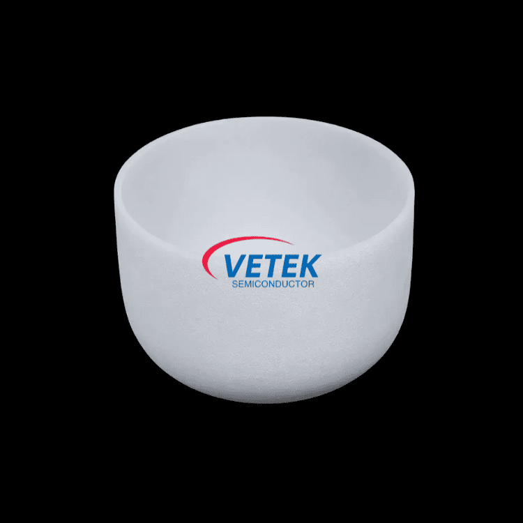
VETEK's CVD SiC coated graphite components are used in SiC Epitaxy Susceptors, MOCVD Carriers, Wafer Carriers, Halfmoon Components, and Semiconductor Thermal Components.
• High-purity SiC coating
• Excellent thermal uniformity
• High-temperature stability
• Strong corrosion resistance

VETEK CVD SiC coated graphite components for SiC epitaxy, MOCVD, and semiconductor thermal applications.
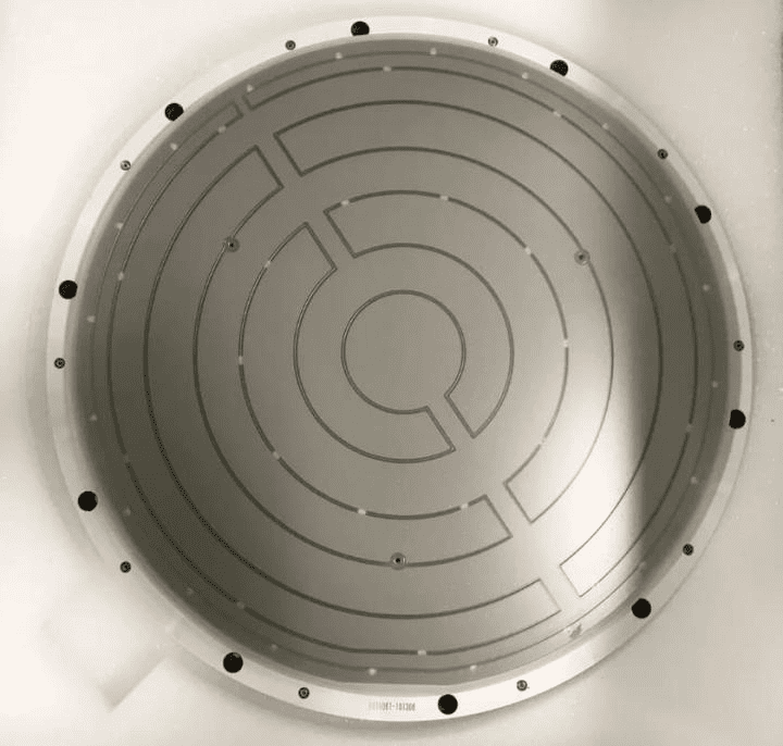
For advanced etch and high-temperature processes, Solid CVD SiC delivers a higher grade of material performance. Typical applications include Focus Rings, RTP/EPI Components, and Plasma Process Components.
• Dense, non-porous structure
• Extremely low particle generation
• Excellent plasma resistance
• Long service life

Solid CVD SiC focus rings and plasma process components for advanced etch and RTP/EPI applications.
As SiC crystal growth temperatures continue to rise, tantalum carbide (TaC) coatings have become an important material for ultra-high-temperature thermal fields. TaC offers higher temperature stability, excellent oxidation resistance, and outstanding chemical stability — suited to SiC crystal growth equipment, high-temperature thermal field components, and third-generation semiconductor manufacturing environments.

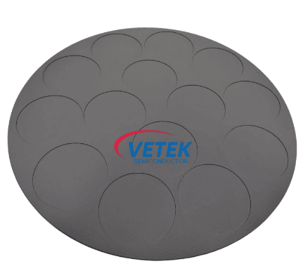
TaC-coated hot-zone components engineered for ultra-high-temperature SiC crystal growth.
Together, these three product lines address the different thermal and chemical demands found across the SiC manufacturing chain:
|
Solution |
Best Suited For |
Key Benefit |
Typical Components |
|
CVD SiC Coated Graphite |
SiC/MOCVD/LED epitaxy, RTP/RTA |
Combines graphite's thermal performance with SiC's corrosion resistance |
Susceptors, wafer carriers, halfmoon components |
|
Solid CVD SiC |
Advanced etch, high-temp plasma processes |
Dense, non-porous, ultra-low particle generation |
Focus rings, RTP/EPI components |
|
TaC Coating |
SiC crystal growth, ultra-high-temp hot zones |
Highest temperature stability and oxidation resistance |
Hot-zone and thermal field components |
SiC epitaxy grows a crystalline silicon carbide layer to make semiconductor wafers and devices. SiC coating (CVD SiC) deposits a thin, dense SiC layer onto graphite or other substrates to protect equipment components from heat and corrosion. They serve different purposes within the same manufacturing chain.
Bare graphite has excellent thermal conductivity and stability, but it corrodes and generates particles when exposed to high temperatures and gases such as H₂ and HCl over time. A dense CVD SiC coating adds hardness, chemical resistance, and high-temperature stability while preserving graphite's thermal performance.
Solid CVD SiC is a fully dense, non-porous silicon carbide material used in advanced etch and high-temperature processes, including focus rings, RTP/EPI components, and plasma process parts — applications that require extremely low particle generation and long service life.
As SiC crystal growth processes push toward higher temperatures, hot-zone components need materials that resist oxidation and stay chemically stable under extreme heat. TaC coatings offer higher temperature stability than graphite alone, making them well suited to SiC crystal growth furnaces and high-temperature thermal field components.
Larger wafers increase the number of dies per wafer, which lowers manufacturing cost per chip and improves scalability. Wafer makers and chipmakers are now qualifying 8-inch SiC substrates and epitaxial wafers to meet growing demand from EVs, renewable energy, and industrial power electronics.
The SiC industry's defining question has changed — from whether the material could be commercialized, to how efficiently, cleanly, and consistently it can be manufactured at scale.
In 2013, the industry's central question was whether SiC could be commercialized at all. Today, more than a decade later, that question has become: how can SiC products be manufactured with higher efficiency, fewer defects, and greater stability?
As the SiC industry continues to expand, larger wafer diameters, upgraded epitaxy technology, and optimized manufacturing equipment remain the core directions of industry development. At the same time, high-purity CVD SiC coatings, Solid CVD SiC, and TaC materials are becoming key technologies for ensuring semiconductor manufacturing stability.
VETEK Semiconductor remains focused on advanced semiconductor materials, providing reliable material solutions for SiC epitaxy, crystal growth, and high-temperature semiconductor manufacturing — supporting the next generation of the semiconductor industry.

VETEK Semiconductor designs and manufactures CVD SiC coated graphite, Solid CVD SiC, and TaC coating components for SiC epitaxy, MOCVD, crystal growth, and high-temperature semiconductor equipment. This article was prepared by VETEK's materials engineering team, drawing on industry reporting from Semiconductor Today and current SiC wafer market analysis, and reflects VETEK's direct experience supplying components into SiC manufacturing lines.
Sources referenced: Semiconductor Today (2013 industry feature); GlobalWafers public statements (2023); Compound Semiconductor News (2024); Patsnap Eureka SiC wafer price analysis (2025). Figures and equipment specifications for VETEK products are based on internal product documentation.
+86-579-87223657
Wangda Road, Ziyang Street, Wuyi County, Jinhua City, Zhejiang Province, China