QR Code

Products
Contact Us


Fax
+86-579-87223657

E-mail

Address
Wangda Road, Ziyang Street, Wuyi County, Jinhua City, Zhejiang Province, China
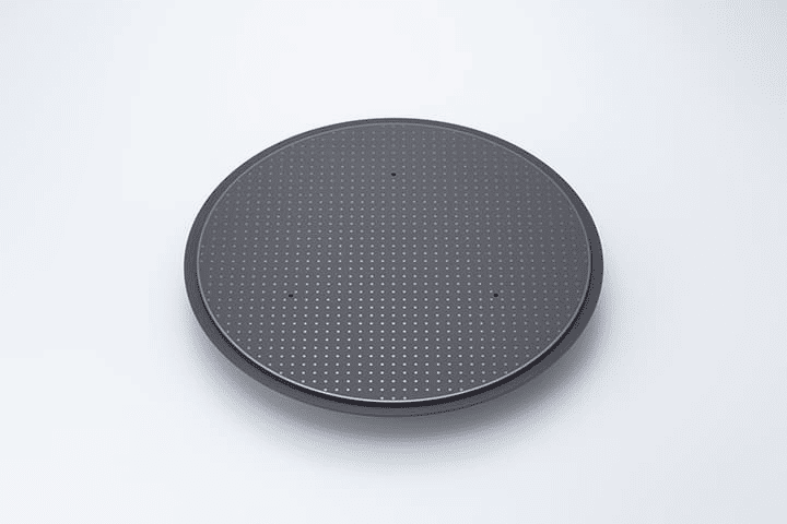
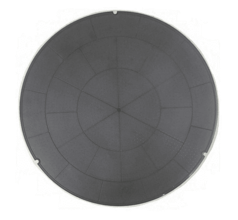
Electrostatic Chuck (ESC for short) is a device that uses electrostatic force to absorb and fix silicon wafers or other substrates. It is widely used in plasma etching (Plasma Etching), chemical vapor deposition (CVD), physical vapor deposition (PVD) and other process links in the vacuum environment of semiconductor manufacturing.
Compared with traditional mechanical fixtures, ESC can firmly fix wafers without mechanical stress and pollution, improve processing accuracy and consistency, and is one of the key equipment components of high-precision semiconductor processes.

Electrostatic chucks can be divided into the following categories according to structural design, electrode materials and adsorption methods:
1. Monopolar ESC
Structure: one electrode layer + one ground plane
Features: Requires auxiliary helium (He) or nitrogen (N₂) as an insulating medium
Application: Suitable for processing high-impedance materials such as SiO₂ and Si₃N₄
2. Bipolar ESC
Structure: two electrodes, the positive and negative electrodes are embedded in the ceramic or polymer layer respectively
Features: It can work without additional media and is suitable for materials with good conductivity
Advantages: Stronger adsorption and faster response
3. Thermal Control (He Backside Cooling ESC)
Function: Combined with the backside cooling system (usually helium), the temperature is precisely controlled while fixing the wafer
Application: Widely used in plasma etching and processes where the etching depth needs to be precisely controlled
4. Ceramic ESC Material:
High insulation ceramic materials such as aluminum oxide (Al₂O₃), aluminum nitride (AlN), and silicon nitride (Si₃N₄) are usually used.
Features: corrosion resistance, excellent insulation performance, and high thermal conductivity.
1. Plasma Etching ESC fixes the wafer in the reaction chamber and realizes back cooling, controlling the wafer temperature within ±1℃, thereby ensuring that the etching rate uniformity (CD Uniformity) is controlled within ±3%.
2. Chemical Vapor Deposition (CVD) ESC can achieve stable adsorption of wafers under high temperature conditions, effectively suppress thermal deformation, and improve the uniformity and adhesion of thin film deposition.
3. Physical Vapor Deposition (PVD) ESC provides contactless fixation to prevent wafer damage caused by mechanical stress, and is particularly suitable for the processing of ultra-thin wafers (<150μm).
4. Ion ImplantationThe temperature control and stable clamping capabilities of ESC prevent local damage to the wafer surface due to charge accumulation, ensuring the accuracy of implantation dose control.
5. Advanced PackagingIn chiplets and 3D IC packaging, ESC is also used in redistribution layers (RDL) and laser processing, supporting the processing of non-standard wafer sizes.

1. Holding Force DegradationProblem description:
After long-term operation, due to electrode aging or ceramic surface contamination, the ESC holding force decreases, causing the wafer to shift or fall off.
Solution: Use plasma cleaning and regular surface treatment.
2. Electrostatic Discharge (ESD) Risk:
High voltage bias may cause instantaneous discharge, damaging the wafer or equipment.
Countermeasures: Design a multi-layer electrode insulation structure and configure an ESD suppression circuit.
3. Temperature Non-Uniformity Reason:
Uneven cooling of the back of the ESC or difference in thermal conductivity of ceramics.
Data: Once the temperature deviation exceeds ±2℃, it may cause an etching depth deviation of >±10%.
Solution: High thermal conductivity ceramics (such as AlN) with high-precision He pressure control system (0–15 Torr).
4. Deposition ContaminationProblem:
Process residues (such as CF₄, SiH₄ decomposition products) are deposited on the surface of the ESC, affecting adsorption capacity.
Countermeasure: Use plasma in-situ cleaning technology and perform routine cleaning after running 1,000 wafers.
User focus
Actual needs
Recommended solutions
Wafer fixation reliability
Prevent wafer slippage or drift during high-temperature processes
Use bipolar ESC
Temperature control accuracy
Controlled at ±1°C to ensure process stability
Thermally controlled ESC, with He cooling system
Corrosion resistance and life
Stable use under high-density plasma processes >5000 h
Ceramic ESC (AlN/Al₂O₃)
Quick response and maintenance convenience
Quick clamping release, easy cleaning and maintenance
Detachable ESC structure
Wafer type compatibility
Supports 200 mm/300 mm/non-circular wafer processing
Modular ESC design


+86-579-87223657


Wangda Road, Ziyang Street, Wuyi County, Jinhua City, Zhejiang Province, China
Copyright © 2024 WuYi TianYao Advanced Material Tech.Co.,Ltd. All Rights Reserved.
Links | Sitemap | RSS | XML | Privacy Policy |
