QR Code

Products
Contact Us


Fax
+86-579-87223657

E-mail

Address
Wangda Road, Ziyang Street, Wuyi County, Jinhua City, Zhejiang Province, China
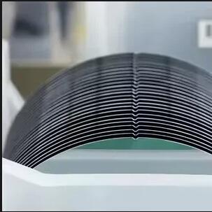
Silicon wafers are the foundation of integrated circuits and semiconductor devices. They have an interesting feature - flat edges or tiny grooves on the sides .It is not a defect, but a deliberately designed functional marker.In fact, this notch serves as a directional reference and identity marker throughout the entire manufacturing process.

In the early days, wafers mostly used a “flat” as the marker, meaning a short straight segment ground on the circular edge. The position and number of these flats were used to distinguish crystal orientations and doping types. As wafer size increased and process precision improved, mainstream 200 mm and 300 mm wafers have largely standardized on a small arc-shaped notch design. The position of this notch is defined by standards and is located at a fixed orientation, used to indicate the wafer’s crystal orientation (for example <100> or <111>) and to provide a common reference point for subsequent equipment.
What is the function of the wafer notch?
For device and process engineers, the notch on a wafer may look insignificant, but it runs through the entire process chain from crystal pulling, epitaxy and wafer fabrication all the way to pre-packaging test. Whenever “direction” is involved—crystal orientation, layout alignment, stress orientation, or even the structure design of certain power devices—this small geometric marker is almost always in the background. Once you understand the role of the notch, it becomes much easier to follow how a wafer “moves” through the production line and how each process step builds its coordinate system around this piece of silicon.


+86-579-87223657


Wangda Road, Ziyang Street, Wuyi County, Jinhua City, Zhejiang Province, China
Copyright © 2024 WuYi TianYao Advanced Material Tech.Co.,Ltd. All Rights Reserved.
Links | Sitemap | RSS | XML | Privacy Policy |
