


 Coated Graphite RTP RTA Carrier")


QR Code

Products
Contact Us


Fax
+86-579-87223657

E-mail

Address
Wangda Road, Ziyang Street, Wuyi County, Jinhua City, Zhejiang Province, China


Chemical mechanical polishing (CMP) removes excess material and surface defects through the combined action of chemical reactions and mechanical abrasion. It is a key process for achieving global planarization of the wafer surface and is indispensable for multilayer copper interconnects and low-k dielectric structures. In practical manufacturing, CMP is not a perfectly uniform removal process; it gives rise to typical pattern-dependent defects, among which dishing and erosion are the most prominent. These defects directly affect the geometry of the interconnect layers and their electrical characteristics.
Dishing refers to the excessive removal of relatively soft conductive materials (such as copper) during CMP, leading to a dish-shaped concave profile inside a single metal line or a large metal area. In cross-section, the center of the metal line lies lower than its two edges and the surrounding dielectric surface. This phenomenon is frequently observed in wide lines, pads, or block-type metal regions. Its formation mechanism is mainly related to differences in material hardness and the deformation of the polishing pad over wide metal features: soft metals are more sensitive to the chemical components and abrasives in the slurry, and the local contact pressure of the pad increases on wide features, causing the removal rate at the center of the metal to exceed that at the edges. As a result, the depth of dishing usually increases with line width and over-polish time.
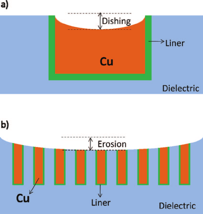
Erosion is characterized by the overall surface height in high pattern-density regions (such as dense metal line arrays or areas with dense dummy fill) being lower than that in surrounding sparse regions after CMP. In essence, it is a pattern-density-driven, region-level over-removal of material. In dense regions, metal and dielectric together provide a larger effective contact area, and the mechanical friction and chemical action of the pad and slurry are stronger. Consequently, the average removal rates of both metal and dielectric are higher than in low-density regions. As polishing and over-polishing proceed, the metal–dielectric stack in dense areas becomes thinner as a whole, forming a measurable height step, and the degree of erosion increases with local pattern density and process loading.
From the perspective of device and process performance, dishing and erosion have multiple adverse impacts on semiconductor products. Dishing reduces the effective cross-sectional area of the metal, leading to higher interconnect resistance and IR drop, which in turn causes signal delay and reduced timing margin on critical paths. Variations in dielectric thickness caused by erosion change the parasitic capacitance between metal lines and the distribution of RC delay, undermining the uniformity of electrical characteristics across the chip. In addition, local dielectric thinning and electric field concentration affect the breakdown behavior and long-term reliability of inter-metal dielectrics. At the integration level, excessive surface topography increases the difficulty of lithography focus and alignment, degrades the uniformity of subsequent film deposition and etching, and may induce defects such as metal residue. These issues ultimately manifest as yield fluctuation and a shrinking process window. Therefore, in practical engineering, it is necessary to control dishing and erosion within specified limits through layout density equalization, optimization of polishing slurry selectivity,and fine tuning of CMP process parameters, so as to ensure the planarity of interconnect structures, stable electrical performance, and robust high-volume manufacturing.
+86-579-87223657
Wangda Road, Ziyang Street, Wuyi County, Jinhua City, Zhejiang Province, China