


 and gallium nitride (GaN) applications? - VeTek Semiconductor")
QR Code

Products
Contact Us


Fax
+86-579-87223657

E-mail

Address
Wangda Road, Ziyang Street, Wuyi County, Jinhua City, Zhejiang Province, China


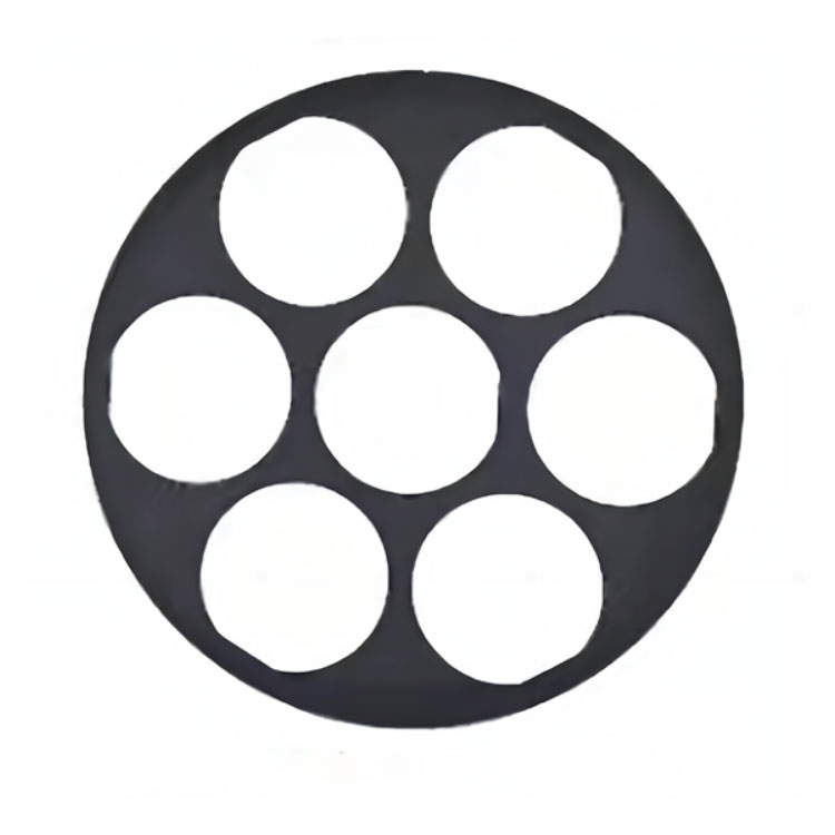
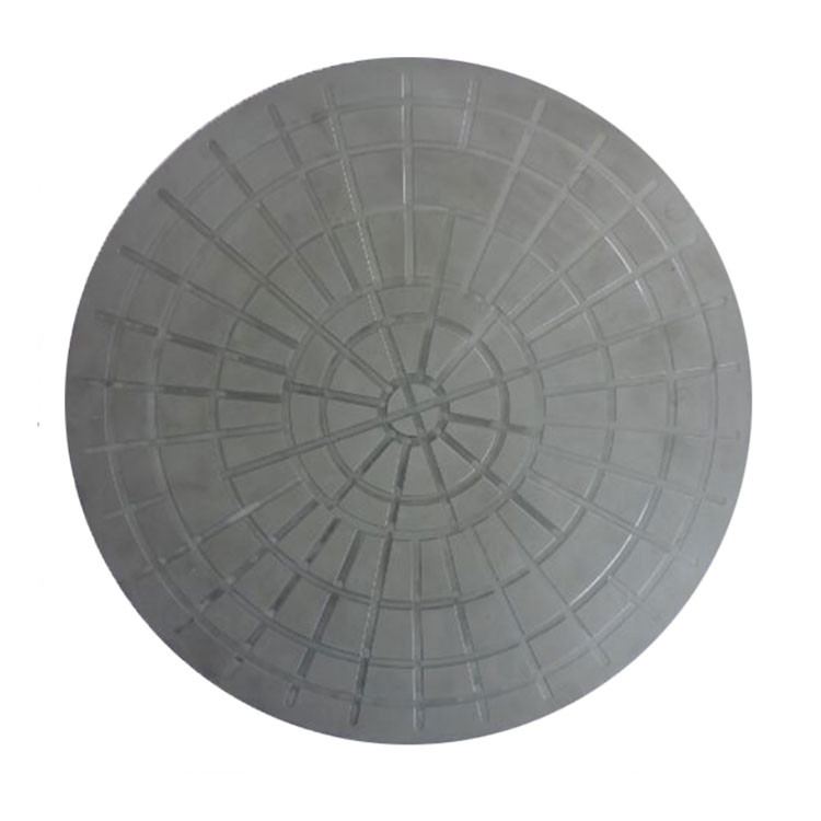
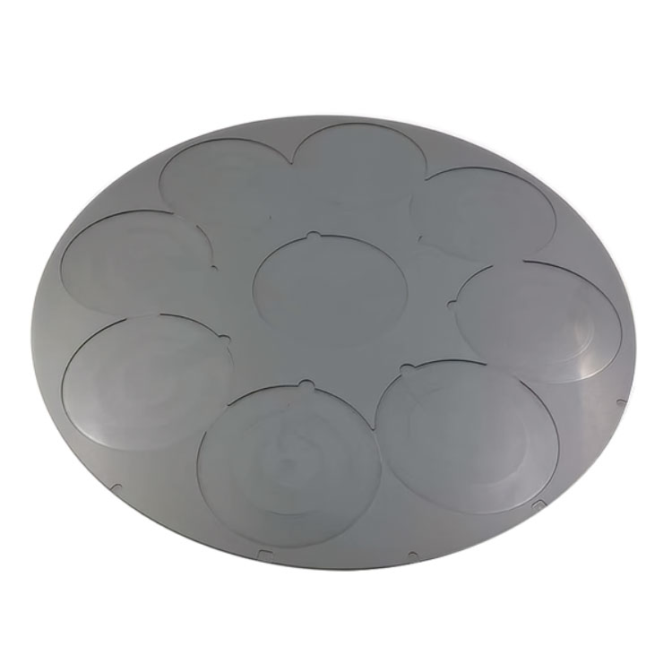
VeTek Semiconductor ICPPSS (Inductively Coupled Plasma Photoresist Stripping) Etching Process Wafer Carrier is specifically designed to meet the demanding requirements of the semiconductor industry's etching processes. With its advanced features, it ensures optimal performance, efficiency, and reliability throughout the etching process.
Enhanced Chemical Compatibility: The wafer carrier is constructed using materials that exhibit excellent chemical compatibility with the etching process chemistries. This ensures compatibility with a wide range of etchants, resist strippers, and cleaning solutions, minimizing the risk of chemical reactions or contamination.
High Temperature Resistance: The wafer carrier is designed to withstand high temperatures encountered during the etching process. It maintains its structural integrity and mechanical strength, preventing deformation or damage even under extreme thermal conditions.
Superior Etch Uniformity: The carrier features a precisely engineered design that promotes uniform distribution of etchants and gases across the wafer surface. This results in consistent etch rates and high-quality, uniform patterns, essential for achieving precise and reliable etching results.
Excellent Wafer Stability: The carrier incorporates a secure wafer holding mechanism that ensures stable positioning and prevents wafer movement or slippage during the etching process. This guarantees accurate and repeatable etch patterns, minimizing defects and yield losses.
Cleanroom Compatibility: The wafer carrier is designed to meet strict cleanroom standards. It features low particle generation and excellent cleanliness, preventing any particle contamination that could compromise the quality and yield of the etching process.Impurity is below 5ppm.
Robust and Durable Construction: The carrier is engineered using high-quality materials known for their durability and long lifespan. It can withstand repeated use and rigorous cleaning processes without compromising its performance or structural integrity.
Customizable Design: We offer customizable options to meet specific customer requirements. The carrier can be tailored to accommodate different wafer sizes, thicknesses, and process specifications, ensuring compatibility with various etching equipment and processes.
Experience the reliability and performance of our ICP/PSS Etching Process Wafer Carrier, designed to optimize the etching process in the semiconductor industry. Its enhanced chemical compatibility, high-temperature resistance, superior etch uniformity, excellent wafer stability, cleanroom compatibility, robust construction, and customizable design make it the ideal choice for your etching applications.


+86-579-87223657
Wangda Road, Ziyang Street, Wuyi County, Jinhua City, Zhejiang Province, China