


QR Code

Products
Contact Us


Fax
+86-579-87223657

E-mail

Address
Wangda Road, Ziyang Street, Wuyi County, Jinhua City, Zhejiang Province, China


Silicon Epitaxy, EPI,Epitaxy,Epitaxial refers to the growth of a layer of crystal with the same crystal direction and different crystal thickness on a single crystalline silicon substrate. Epitaxial growth technology is required for the manufacturing of semiconductor discrete components and integrated circuits, because the impurities contained in semiconductors include N-type and P-type. Through a combination of different types, semiconductor devices exhibit a variety of functions.
Silicon epitaxy growth method can be divided into gas phase epitaxy, liquid phase epitaxy(LPE), solid phase epitaxy, chemical vapor deposition growth method is widely used in the world to meet the lattice integrity.
Typical silicon epitaxial equipment is represented by the Italian company LPE, which has pancake epitaxial hy pnotic tor,barrel type hy pnotic tor,semiconductor hy pnotic,wafer carrier and so on. The schematic diagram of barrel-shaped epitaxial hy pelector reaction chamber is as follows. VeTek Semiconductor can provide barrel-shaped wafer epitaxial hy pelector. The quality of SiC coated HY pelector is very mature. Quality equivalent to SGL; At the same time, VeTek Semiconductor can also provide silicon epitaxial reaction cavity quartz nozzle, quartz Baffle,bell jar and other complete products.

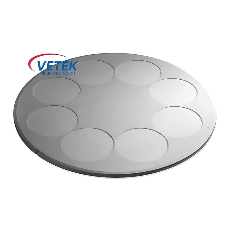
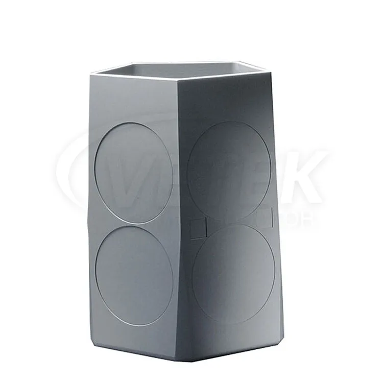 SiC Coated Graphite Barrel Susceptor for EPI
 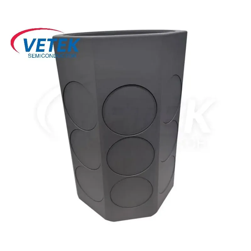 SiC Coated Barrel Susceptor
 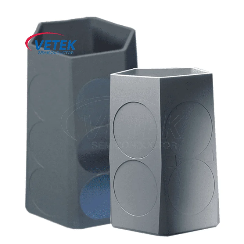 CVD SiC Coated Barrel Susceptor
 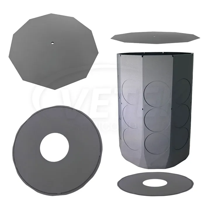 LPE SI EPI Susceptor Set

 SiC coating Monocrystalline silicon epitaxial tray
 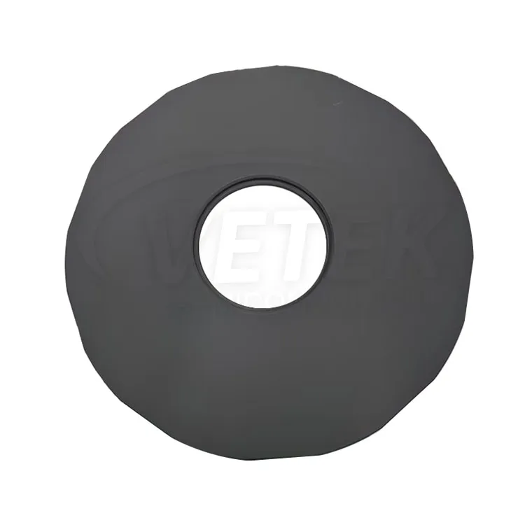 SiC Coated Support for LPE PE2061S
 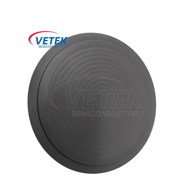 Graphite Rotating Susceptor
 Coated Graphite Shower Head")


Veteksemicon silicon epitaxy solutions are your strategic procurement choice for advanced semiconductor wafer processing, particularly in CMOS, power devices, and MEMS applications. As a key process in wafer engineering, silicon epitaxy (Si Epi) involves the precise deposition of a crystalline silicon layer on top of a polished silicon wafer, offering superior control of doping profiles, defect density, and layer thickness.
Veteksemicon provides epitaxy-ready susceptor parts and reactor components used in Epi CVD systems, supporting both atmospheric and reduced pressure processes. Our product lineup includes silicon epitaxy susceptors, carrier rings, and coated wafer holders, optimized for compatibility with tools from Applied Materials, ASM, and Tokyo Electron (TEL).
Silicon epitaxy plays a critical role in producing ultra-thin junctions, strained silicon layers, and high-voltage isolation structures. Our materials and parts are engineered for high-purity, uniform thermal distribution, and anti-contamination performance during n-type and p-type epitaxial growth.
Closely associated terms include epitaxial wafer, in-situ doping, epitaxy-ready SiC coatings, and epi reactor parts, which support the entire upstream and downstream process of silicon-based IC fabrication.
Discover more about Veteksemicon’s silicon epitaxy support solutions by visiting our product detail page or contacting us for technical consultation and part customization.
+86-579-87223657
Wangda Road, Ziyang Street, Wuyi County, Jinhua City, Zhejiang Province, China