News

News

We are glad to share with you about the results of our work, company news,and give you timely developments and personnel appointment and removal conditions.
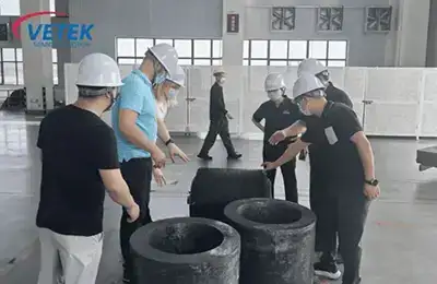
Inside VETEK CNC Precision Machining Workshop: Building the Foundation of High-Purity Semiconductor Components23 2026-09

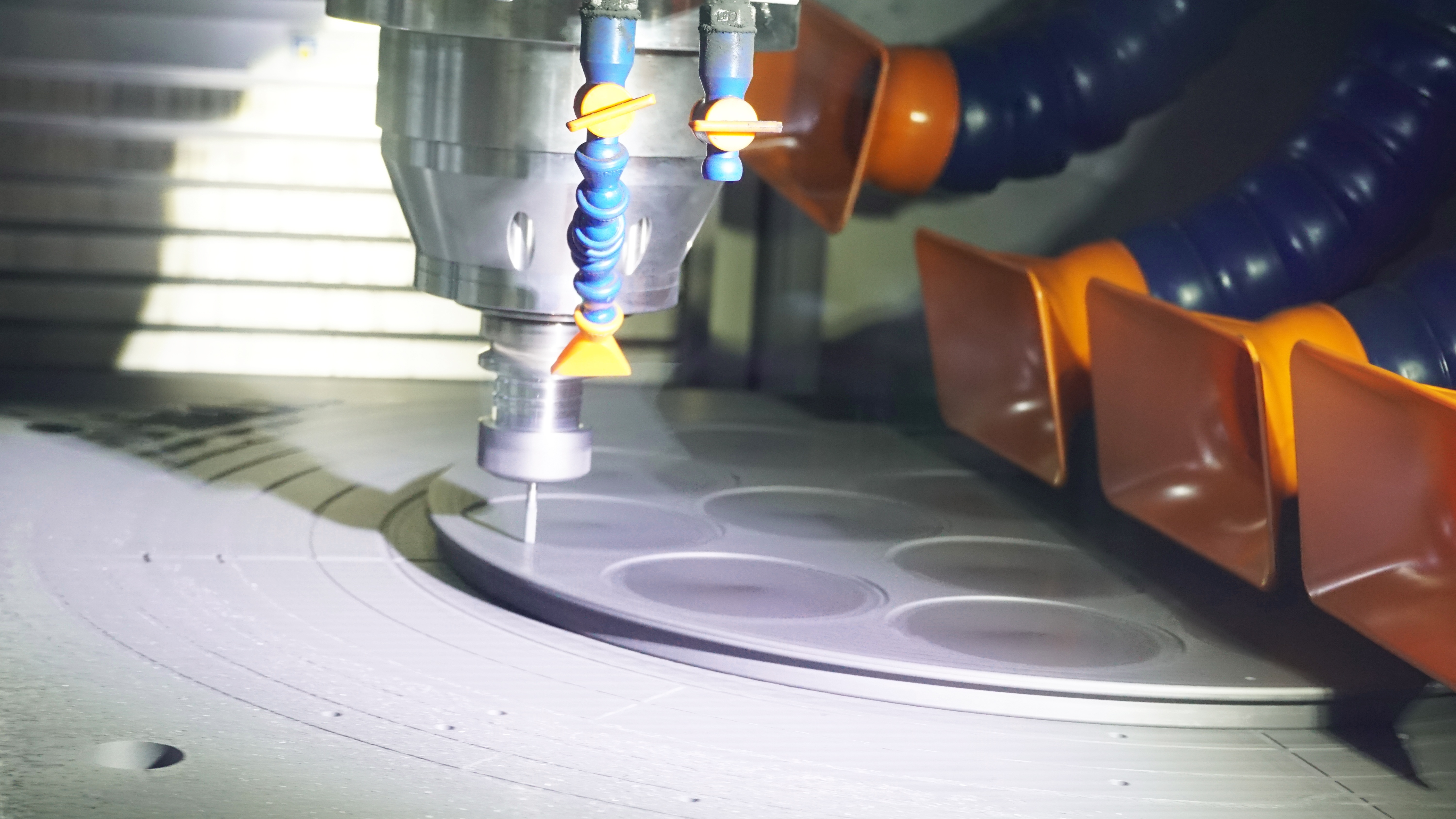
Inside VETEK CNC Precision Machining Workshop: Building the Foundation of High-Purity Semiconductor Components

Discover VeTek Semiconductor’s CNC precision machining capabilities for high-purity graphite, CVD SiC/TaC coated components, solid SiC parts, and custom semiconductor solutions.
Vetek Semiconductor at CSEAC 2026: Advancing Semiconductor Materials, Core Components and Global Collaboration04 2026-09

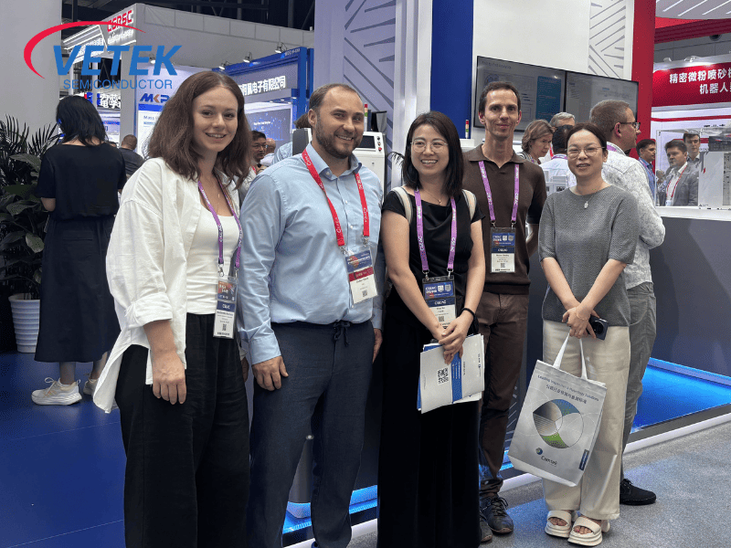
Vetek Semiconductor at CSEAC 2026: Advancing Semiconductor Materials, Core Components and Global Collaboration

Vetek Semiconductor participated in CSEAC 2026 in Wuxi, China, showcasing its advanced CVD SiC and TaC coatings, graphite components, SiC ceramics and other semiconductor core materials. The event provided valuable opportunities to strengthen customer partnerships, discuss new technologies, advance cooperation projects and explore future opportunities across the global semiconductor industry.
VETEK Semiconductor | Manufacturer of CVD SiC/TaC Coatings, Solid SiC, and Critical Semiconductor Materials23 2026-07

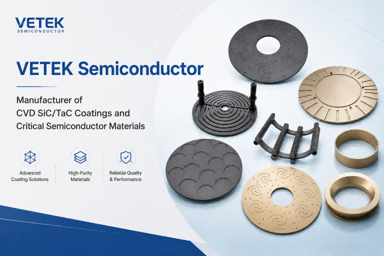
VETEK Semiconductor | Manufacturer of CVD SiC/TaC Coatings, Solid SiC, and Critical Semiconductor Materials

VETEK Semiconductor specializes in six major product categories, including CVD SiC coatings, CVD TaC coatings, Solid SiC, high-purity graphite and carbon fiber, quartz and advanced ceramics, and semiconductor wafers. Our products serve critical semiconductor processes such as epitaxy, etching, and crystal growth. With dual R&D platforms, a fully integrated manufacturing system, and global supply capabilities, we are recognized as a National Specialized and Sophisticated "Little Giant" Enterprise.
VETEK New Semiconductor Manufacturing Base Enters Cleanroom Construction Phase13 2026-06

VETEK New Semiconductor Manufacturing Base Enters Cleanroom Construction Phase

VETEK's new semiconductor manufacturing facility has entered the semiconductor-grade cleanroom construction stage. The new site will support the production of CVD SiC coated graphite components, TaC coatings, PyC coatings, Solid SiC parts, and high-purity graphite materials for semiconductor applications.
VeTek Semiconductor at SNEC 2026 Shanghai: Advancing Materials for Next-Generation Solar Manufacturing05 2026-06

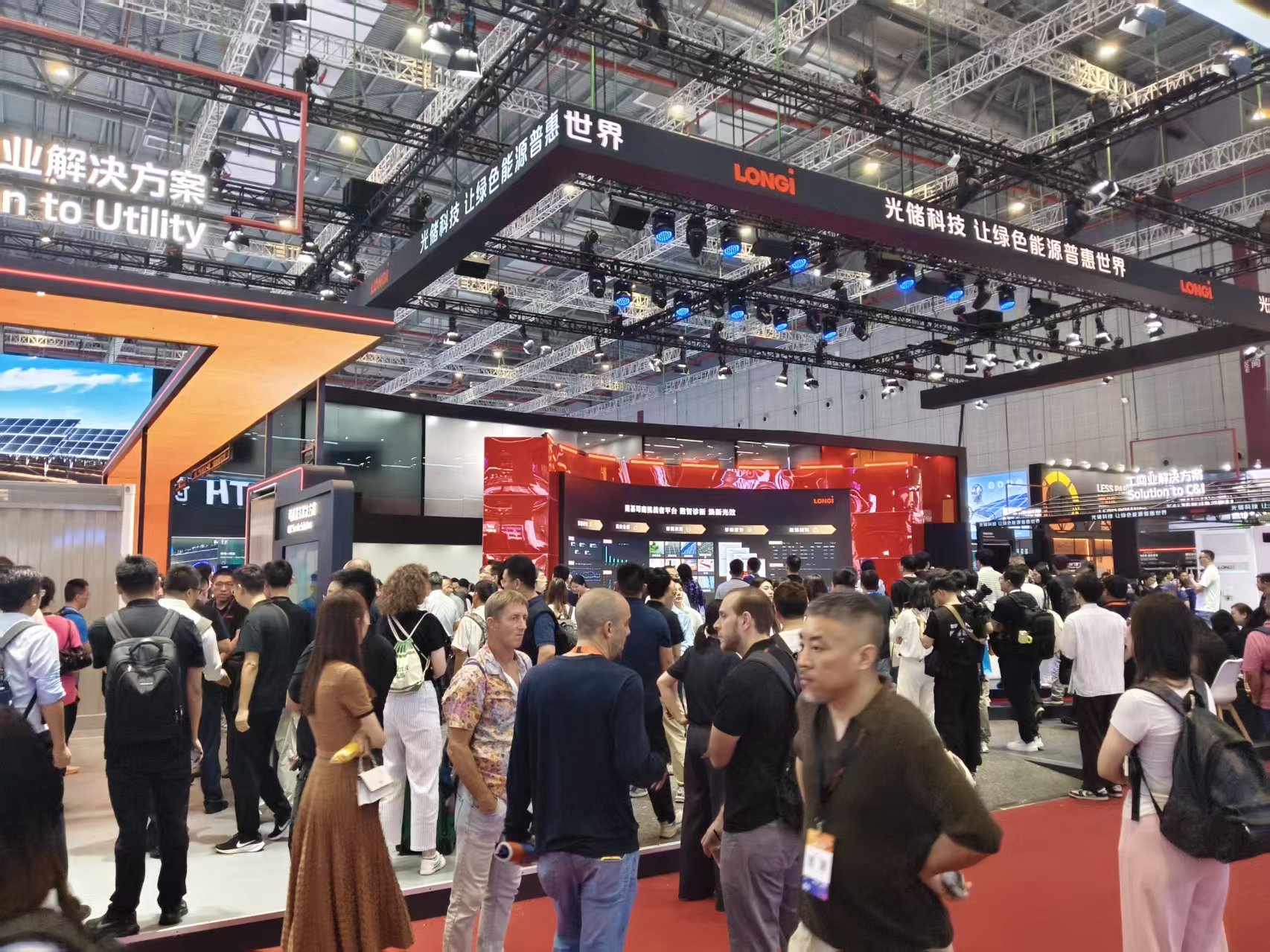
VeTek Semiconductor at SNEC 2026 Shanghai: Advancing Materials for Next-Generation Solar Manufacturing

VeTek Semiconductor shares key insights from SNEC 2026 Shanghai, highlighting high-purity graphite, CVD SiC coated graphite components, carbon composites, and advanced thermal field materials supporting next-generation solar manufacturing and photovoltaic production.
VETEK Celebrates Topping-Out Ceremony of New Semiconductor Manufacturing Base29 2026-05

VETEK Celebrates Topping-Out Ceremony of New Semiconductor Manufacturing Base

VETEK celebrates the topping-out ceremony of its new semiconductor manufacturing base, expanding production capacity for advanced SiC, TaC and PyC coating technologies, Solid SiC components, high-purity graphite parts and semiconductor thermal field materials.
Welcome customers to visit Veteksemicon's SiC Coating/ TaC Coating and Epitaxy Process Factory05 2024-09

Welcome customers to visit Veteksemicon's SiC Coating/ TaC Coating and Epitaxy Process Factory

On September 5, VeTek Semiconductor's customers visited the SiC Coating and TaC Coating factories and reached further agreements on the latest Epitaxial Process solutions.
Welcome Customers to Visit Veteksemicon's Carbon Fiber Products Factory10 2025-09

Welcome Customers to Visit Veteksemicon's Carbon Fiber Products Factory

On September 5, 2025, a customer from Poland visited a factory under VETEK to learn about our advanced technologies and innovative processes in the production of carbon fiber products.
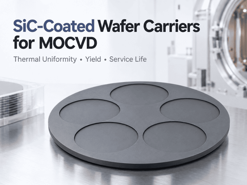
SiC-Coated Wafer Carriers for MOCVD: Thermal Uniformity, Yield and Service Life30 2026-09

SiC-Coated Wafer Carriers for MOCVD: Thermal Uniformity, Yield and Service Life

SiC-coated graphite wafer carriers are critical thermal and mechanical components in MOCVD systems for GaN and LED epitaxy. This technical article explains how carrier geometry, pocket depth, flatness, graphite properties and CVD SiC coating condition influence wafer temperature distribution, epitaxial uniformity and process repeatability. It also examines the relationship between thermal uniformity and device yield, common coating degradation mechanisms, service-life considerations and the engineering data required when specifying a custom or replacement MOCVD wafer carrier.
Why Is Graphite Coated with Silicon Carbide for Semiconductor Epitaxy?18 2026-09

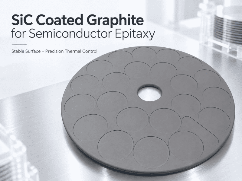
Why Is Graphite Coated with Silicon Carbide for Semiconductor Epitaxy?

SiC-coated graphite combines the machinability and thermal behavior of high-purity graphite with a chemically stable CVD silicon carbide process surface. This technical white paper explains why bare graphite can become a source of chemical interaction, impurities and particles in epitaxy reactors, how CVD SiC creates a more stable process boundary, and why coating integrity, substrate compatibility, geometry and thermal behavior must be engineered together. It also examines the different demands of silicon and SiC epitaxy and outlines how coated susceptors should be specified for semiconductor applications.
SiC-Coated Graphite Susceptor: How It Affects Epitaxy Uniformity and Wafer Quality?18 2026-09

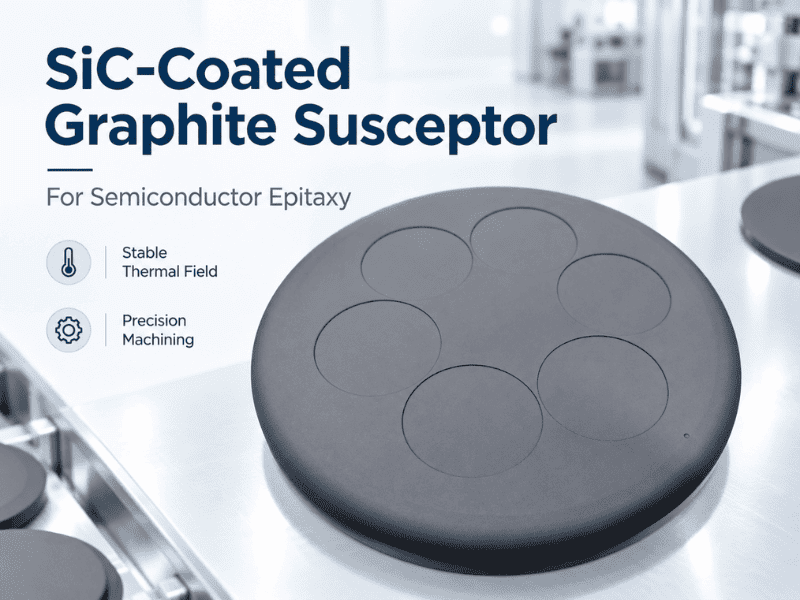
SiC-Coated Graphite Susceptor: How It Affects Epitaxy Uniformity and Wafer Quality?

A SiC-coated graphite susceptor is a critical thermal-field component in semiconductor epitaxy rather than simply a wafer holder. This technical article explains how susceptor geometry, flatness, pocket design, graphite properties and CVD SiC coating quality work together to influence wafer thermal boundaries, temperature distribution and epitaxial uniformity. It also examines common susceptor failure modes, coating degradation, particle risks and the key engineering parameters required when specifying a custom or replacement epitaxy susceptor.
How Is CVD Silicon Carbide Coating Deposited on Graphite?10 2026-09

How Is CVD Silicon Carbide Coating Deposited on Graphite?

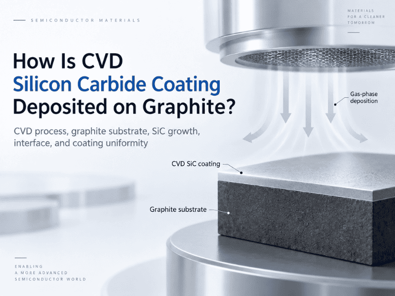
CVD silicon carbide coating is produced by depositing a dense SiC layer onto high-purity graphite through controlled gas-phase and surface reactions. This article explains substrate preparation, MTS-based CVD growth, nucleation and mass transfer, coating thickness and uniformity, SiC/graphite interface stress, common defects and semiconductor-grade inspection. It also shows why process parameters and component geometry must be engineered together for susceptors and wafer carriers used in epitaxy and MOCVD.
What Is Silicon Carbide (SiC) Coating? Properties, CVD Process & Applications09 2026-09

What Is Silicon Carbide (SiC) Coating? Properties, CVD Process & Applications

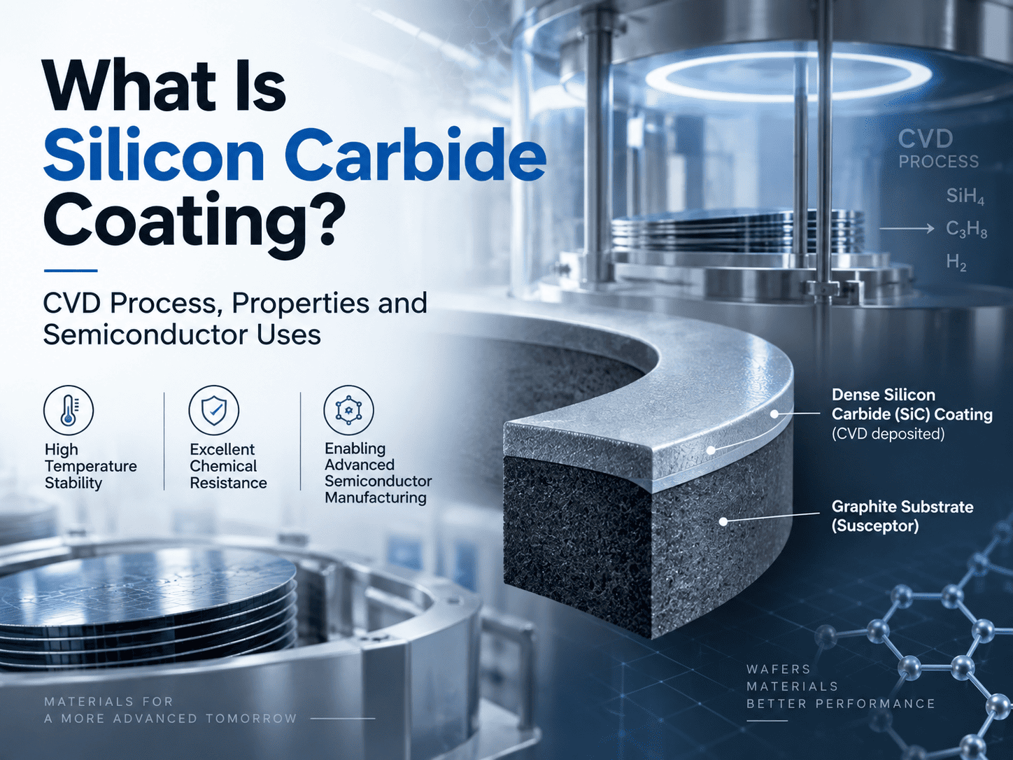
Silicon carbide coating is a dense CVD SiC layer applied to high-purity graphite components used in semiconductor processing. This article explains why graphite is coated with SiC, how CVD SiC is formed, which coating properties and interface factors control performance, and how SiC-coated graphite supports silicon epitaxy, SiC epitaxy and MOCVD. It also examines coating thickness, CTE mismatch, delamination risk and the engineering information required when specifying susceptors, wafer carriers and other coated components.
CVD Coatings in Semiconductor Epitaxy: Engineering Parameters, SiC/TaC Selection and Failure Control04 2026-09

CVD Coatings in Semiconductor Epitaxy: Engineering Parameters, SiC/TaC Selection and Failure Control

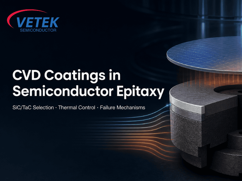
Technical white paper on how CVD SiC and TaC coatings influence thermal stability, contamination, particles and repeatability in semiconductor epitaxy, with parameter tables, a coating-selection decision tree, failure mechanisms and RFQ criteria.
TaC Coating: The Gatekeeper of Yield for 8-inch Silicon Carbide PVT Epitaxy28 2026-08

TaC Coating: The Gatekeeper of Yield for 8-inch Silicon Carbide PVT Epitaxy

8-inch SiC is now in volume production, but wafer yield — not capacity — separates the winners. This guide explains why TaC coating on graphite hot-zone parts decides yield, and how to qualify a supplier.
Substrate vs. Epitaxy: Key Roles in Semiconductor Manufacturing21 2026-08

Substrate vs. Epitaxy: Key Roles in Semiconductor Manufacturing

In modern chip manufacturing, the substrate provides physical support and a heat dissipation path, while the epitaxial layer determines the electrical performance limits of the device. This article provides an in-depth analysis of the fundamental differences between single-crystal silicon and silicon carbide substrates and CVD/MBE epitaxial processes, and reveals how epitaxial technology enhances the performance of high-frequency and high-voltage devices by reducing defect density and incorporating strain engineering. Whether you are a process engineer or a procurement decision-maker, this guide will help you quickly identify the most suitable wafer selection strategy.
X
We use cookies to offer you a better browsing experience, analyze site traffic and personalize content. By using this site, you agree to our use of cookies. Privacy Policy
RejectAccept