We are glad to share with you about the results of our work, company news,and give you timely developments and personnel appointment and removal conditions.
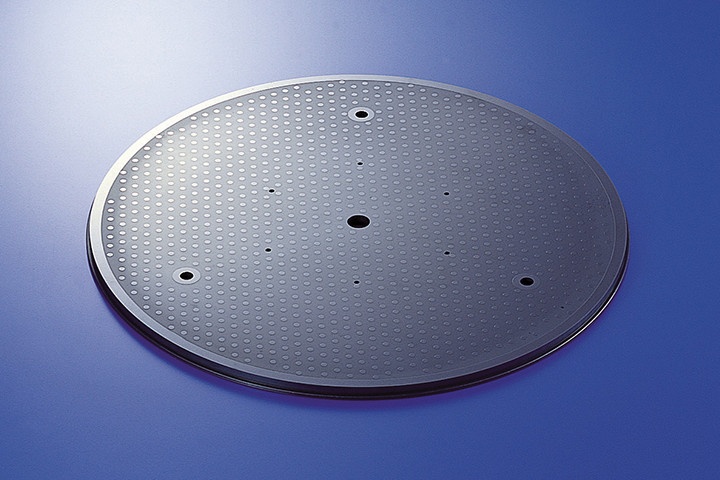
At Veteksemicon, we navigate these challenges daily, specializing in transforming advanced Aluminum Oxide Ceramics into solutions that meet exacting specifications. Understanding the right machining and processing methods is crucial, as the wrong approach can lead to costly waste and component failure. Let’s explore the professional techniques that make this possible.
Introducing CO₂ into the dicing water during wafer cutting is an effective process measure to suppress static charge buildup and lower contamination risk, thereby improving dicing yield and long-term chip reliability.
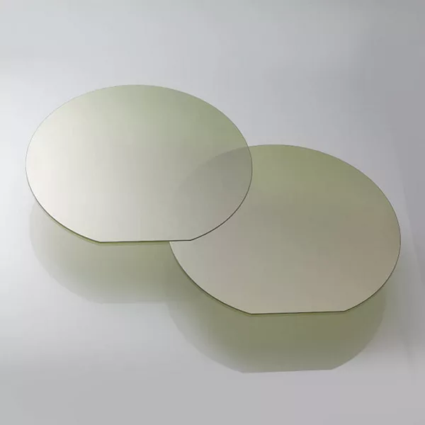
Silicon wafers are the foundation of integrated circuits and semiconductor devices. They have an interesting feature - flat edges or tiny grooves on the sides .It is not a defect, but a deliberately designed functional marker.In fact, this notch serves as a directional reference and identity marker throughout the entire manufacturing process.
Chemical mechanical polishing (CMP) removes excess material and surface defects through the combined action of chemical reactions and mechanical abrasion. It is a key process for achieving global planarization of the wafer surface and is indispensable for multilayer copper interconnects and low-k dielectric structures. In practical manufacturing
Silicon wafer CMP (Chemical Mechanical Planarization) polishing slurry is a critical component in the semiconductor manufacturing process. It plays a pivotal role in ensuring that silicon wafers—used to create integrated circuits (ICs) and microchips—are polished to the exact level of smoothness required for the next stages of production
We use cookies to offer you a better browsing experience, analyze site traffic and personalize content. By using this site, you agree to our use of cookies.
Privacy Policy