We are glad to share with you about the results of our work, company news,and give you timely developments and personnel appointment and removal conditions.
Tantalum carbide (TaC) coatings are widely used in the semiconductor field, mainly for epitaxial growth reactor components, single crystal growth key components, high-temperature industrial components, MOCVD system heaters and wafer carriers.Its excellent high temperature resistance and corrosion resistance can improve equipment durability, yield and crystal quality, reduce energy consumption and improve stability.
During the SiC epitaxial growth process, SiC coated graphite suspension failure may occur. This paper conducts a rigorous analysis of the failure phenomenon of SiC coated graphite suspension, which mainly includes two factors: SiC epitaxial gas failure and SiC coating failure.
This article mainly discusses the respective process advantages and differences of Molecular Beam Epitaxy process and Metal-organic chemical vapour deposition technologies.
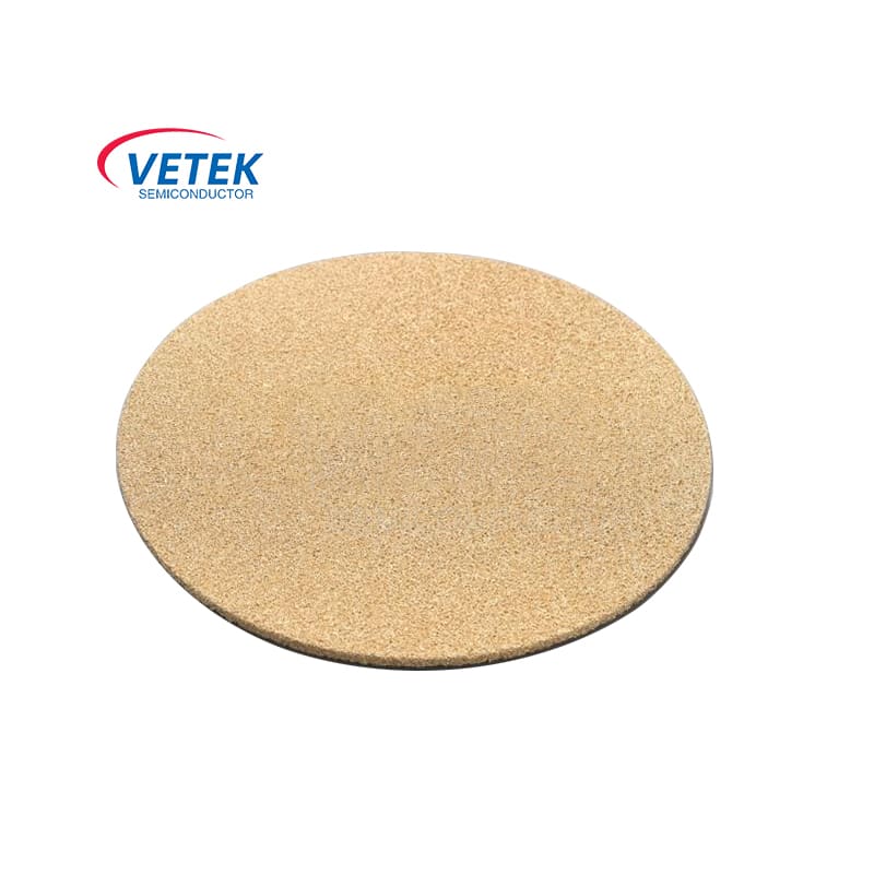
VeTek Semiconductor's Porous Tantalum Carbide, as a new generation of SiC crystal growth material, has many excellent product properties and plays a key role in a variety of semiconductor processing technologies.
The working principle of the epitaxial furnace is to deposit semiconductor materials on a substrate under high temperature and high pressure. Silicon epitaxial growth is to grow a layer of crystal with the same crystal orientation as the substrate and different thickness on a silicon single crystal substrate with a certain crystal orientation. This article mainly introduces the silicon epitaxial growth methods: vapor phase epitaxy and liquid phase epitaxy.
Chemical vapor deposition (CVD) in semiconductor manufacturing is used to deposit thin film materials in the chamber, including SiO2, SiN, etc., and commonly used types include PECVD and LPCVD. By adjusting the temperature, pressure and reaction gas type, CVD achieves high purity, uniformity and good film coverage to meet different process requirements.
This article mainly describes the broad application prospects of silicon carbide ceramics. It also focuses on the analysis of the causes of sintering cracks in silicon carbide ceramics and the corresponding solutions.
Etching technology in semiconductor manufacturing often encounters problems such as loading effect, micro-groove effect and charging effect, which affect product quality. Improvement solutions include optimizing plasma density, adjusting reaction gas composition, improving vacuum system efficiency, designing reasonable lithography layout, and selecting appropriate etching mask materials and process conditions.
Hot pressing sintering is the main method for preparing high-performance SiC ceramics. The process of hot pressing sintering includes: selecting high-purity SiC powder, pressing and molding under high temperature and high pressure, and then sintering. SiC ceramics prepared by this method have the advantages of high purity and high density, and are widely used in grinding discs and heat treatment equipment for wafer processing.
Silicon carbide (SiC)'s Key growth methods include PVT, TSSG, and HTCVD, each with distinct advantages and challenges. Carbon-based thermal field materials like insulation systems, crucibles, TaC coatings, and porous graphite enhance crystal growth by providing stability, thermal conductivity, and purity, essential for SiC's precise fabrication and application.
SiC has high hardness, thermal conductivity, and corrosion resistance, making it ideal for semiconductor manufacturing. CVD SiC coating is created through chemical vapor deposition, providing high thermal conductivity, chemical stability, and a matching lattice constant for epitaxial growth. Its low thermal expansion and high hardness ensure durability and precision, making it essential in applications like wafer carriers, preheating rings, and more. VeTek Semiconductor specializes in custom SiC coatings for diverse industry needs.
Silicon carbide (SiC) is a high-precision semiconductor material known for its excellent properties like high temperature resistance, corrosion resistance, and high mechanical strength. It has over 200 crystal structures, with 3C-SiC being the only cubic type, offering superior natural sphericity and densification compared to other types. 3C-SiC stands out for its high electron mobility, making it ideal for MOSFETs in power electronics. Additionally, it shows great potential in nanoelectronics, blue LEDs, and sensors.
Diamond, a potential fourth-generation "ultimate semiconductor," is gaining attention in semiconductor substrates due to its exceptional hardness, thermal conductivity, and electrical properties. While its high cost and production challenges limit its use, CVD is the preferred method. Despite doping and large-area crystal challenges, diamond holds promise.
SiC and GaN are wide bandgap semiconductors with advantages over silicon, such as higher breakdown voltages, faster switching speeds, and superior efficiency. SiC is better for high-voltage, high-power applications due to its higher thermal conductivity, while GaN excels in high-frequency applications thanks to its superior electron mobility.
Electron beam evaporation is a highly efficient and widely used coating method compared to resistance heating, which heats the evaporation material with an electron beam, causing it to vaporize and condense into a thin film.
We use cookies to offer you a better browsing experience, analyze site traffic and personalize content. By using this site, you agree to our use of cookies. Privacy Policy