


QR Code

Products
Contact Us


Fax
+86-579-87223657

E-mail

Address
Wangda Road, Ziyang Street, Wuyi County, Jinhua City, Zhejiang Province, China


The environment inside a SiC crystal growth furnace is among the least forgiving in semiconductor manufacturing: temperatures exceed 2400°C, hydrogen and ammonia concentrations run high, and graphite components are constantly at risk of shedding particles and releasing impurities. Process engineers have long sought a material solution that can simultaneously withstand extreme heat, aggressive chemistry, and contamination.
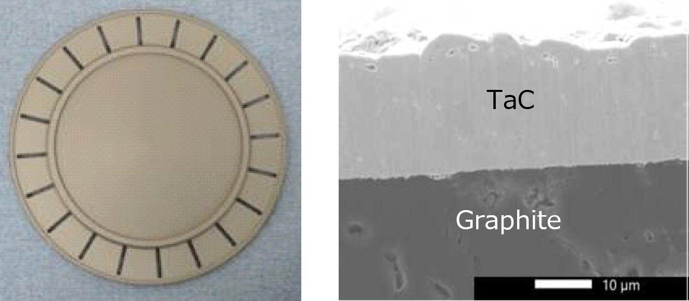
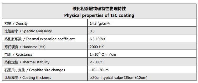
In essence, CVD TaC coating is a protective layer of tantalum carbide (TaC) — a ceramic compound with a distinctive golden-yellow appearance — deposited onto high-purity graphite substrates using chemical vapor deposition. The material itself brings a combination of properties that are hard to find together: a melting point of 3880°C, hardness in the range of 15–19 GPa, strong chemical inertness, and a resistance to corrosion that holds up well in aggressive process environments.
Among the various ways to produce TaC coatings, CVD remains the most mature route. The typical recipe, as detailed, starts with tantalum pentachloride (TaCl₅) and propylene (C₃H₆) as the tantalum and carbon precursors, carried by argon and hydrogen into a heated chamber. Once the vaporized TaCl₅ reaches the graphite surface, it adsorbs and undergoes a sequence of decomposition and recombination reactions. What forms is not just a surface layer, but a dense, well-adhered coating that is notably more uniform and compositionally controllable than what can be achieved with alternative methods like molten salt or sol-gel processing.
2.1 Extremely high thermal stability
CVD TaC coating melts at 3880°C, so it stays structurally sound even above 2200°C. That makes it a good fit for demanding semiconductor processes like SiC crystal growth and MOCVD – places where regular SiC coatings tend to degrade when things get too hot.
2.2 Outstanding chemical corrosion resistance
This coating holds up well against corrosive process gases like hydrogen, ammonia, chlorides, and silicon vapor. Compared to SiC coatings, it cuts down on graphite degradation and particle contamination in high-temperature semiconductor environments. The result? Better process stability and higher wafer yield.
2.3 Good mechanical hardness and thermal shock resistance
CVD TaC coating is hard and bonds strongly to graphite substrates, so it wears slowly and handles thermal shocks nicely. It can take repeated rapid heating and cooling cycles without cracking or peeling off. That means longer component life and faster process ramp rates.
2.4 Ultra‑high purity and impurity suppression
TaC coating has very low impurity levels and acts as a solid diffusion barrier – it stops contaminants from migrating out of the graphite substrate and into the growth environment. This helps cut down crystal defects, keeps impurities out, and improves both the quality and resistivity of SiC crystals.
3.1 SiC Single Crystal Growth (PVT Method)
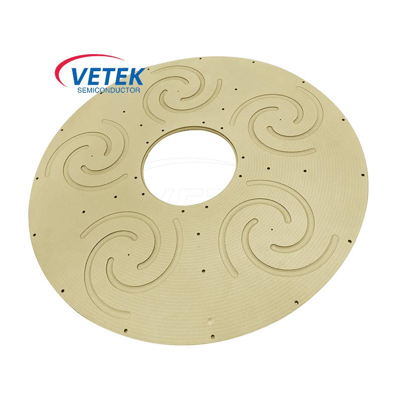
In the PVT growth process of SiC single crystals, TaC coating is applied to key graphite components such as crucibles, guide rings, and seed crystal holders. Research by Fan et al. indicates that TaC coating not only provides physical protection but also, through its low emissivity characteristics, regulates the temperature gradient at the crystal growth interface, improves radial temperature uniformity, maintains SiC sublimation stoichiometry, suppresses impurity migration, and reduces energy consumption. Research by Meng et al. in the Journal of Crystal Growth further confirms that the crystal ingot grown using a crucible structure with a TaC-coated graphite relay ring and graphite paper exhibits superior characteristics in crystal perfection and interface shape. Actual measurements show that the diameter deviation of crystal ingots grown with TaC-coated crucibles is ≤2%, and the crystal surface flatness (RMS) is improved by 40%.
3.2 GaN/SiC Epitaxial Growth
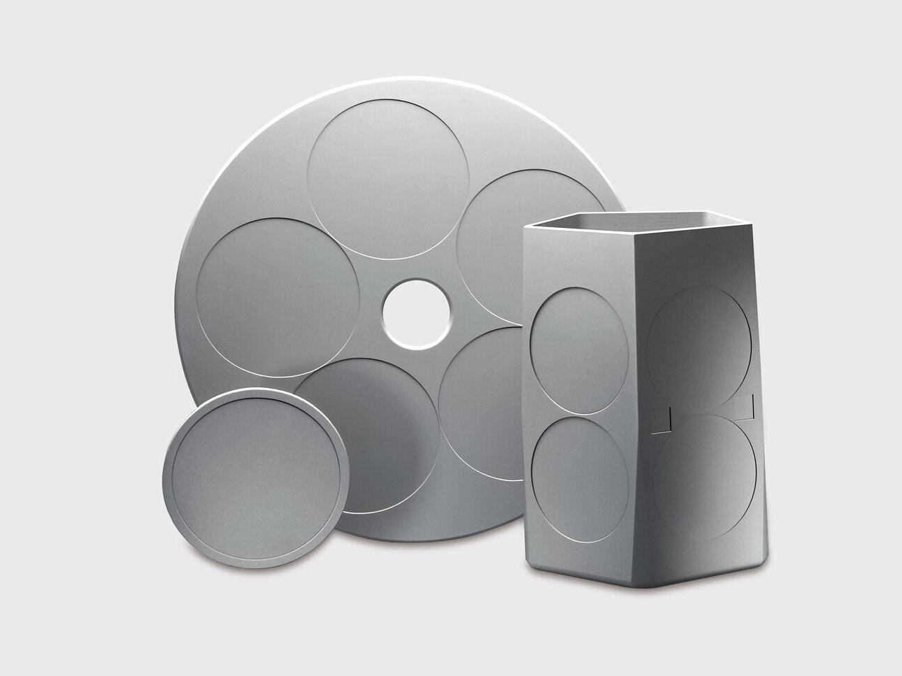
In the CVD reaction chambers for GaN and SiC epitaxy, TaC coating is widely applied to components such as wafer carriers, satellite discs, nozzles, and sensors. These components need to operate for long periods in high-temperature and corrosive environments, and TaC coating can significantly extend their service life and improve process yield. In MOCVD equipment such as Aixtron G5, TaC coating has been proven to be a key material for ensuring process stability.
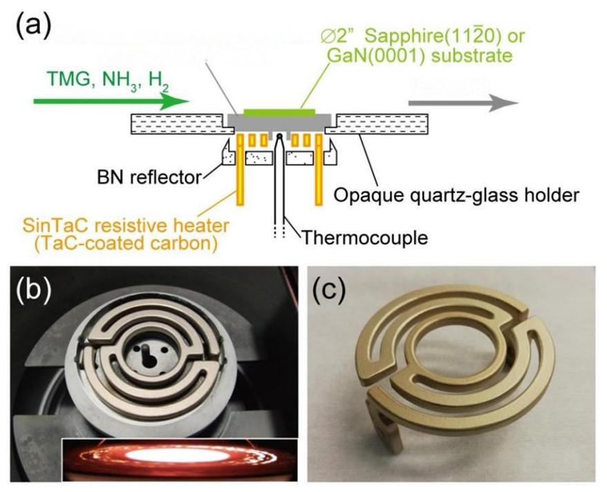
3.3 MOCVD System Heaters
TaC-coated graphite heaters have been successfully applied in MOCVD systems. Compared to traditional pBN-coated heaters, TaC heaters provide better heating efficiency and uniformity, reduce power consumption, and, due to their lower surface emissivity (0.3), help improve thermal field integrity. According to research by Fan et al., the low emissivity of TaC coating not only improves temperature uniformity for crystal growth but also enhances the quality of GaN epitaxial deposition.
3.4 High-Temperature Industrial Applications
Beyond the semiconductor field, TaC coating can also be used for high-temperature industrial components such as resistance heating elements, injection nozzles, shield rings, and brazing fixtures, fully leveraging its comprehensive advantages in heat resistance and corrosion resistance.
In the semiconductor industry, CVD SiC and CVD TaC are the two most mainstream protective coatings for graphite components. The choice depends on specific process temperature requirements.
CVD SiC Coating: Low coefficient of thermal expansion, good structural stability, and cost advantages in environments below 1800°C, widely used in medium-to-high temperature scenarios such as LED epitaxial trays and monocrystalline silicon epitaxial trays.
CVD TaC Coating: Higher thermal stability (melting point 3880°C vs. ~2700°C for SiC), stronger chemical inertness, especially suitable for ultra-high-temperature and highly corrosive environments above 2000°C, such as SiC single crystal growth and GaN epitaxy.
Simply put: When process temperatures exceed 1800°C, especially when corrosive gases such as hydrogen and ammonia are involved, TaC coating is the superior choice.
The rapid expansion of SiC single crystal growth and epitaxy is pulling demand for TaC coatings sharply upward. Two recent market studies point to a market on the verge of significant scale-up. QYResearch, in its Global TaC Coating Market Outlook, In‑Depth Analysis & Forecast to 2031, pegs the 2024 global tantalum carbide coating market at around USD 45 million and projects it will reach USD 142 million by 2031 — a compound annual growth rate of 17.9%. Global Info Research’s figures land in the same range, estimating the 2024 market at roughly USD 47 million and forecasting a climb to USD 143 million by 2031, which works out to a CAGR of 17.5%. The consistency between these forecasts gives confidence that TaC coating is entering a sustained growth phase.
As for who is supplying this market, it remains fairly concentrated at the top. Momentive Technologies, Tokai Carbon, and Toyo Tanso together account for about 76% of global revenue [10]. Geographically, North America leads with roughly 45% of the market, while Asia-Pacific is close behind at around 41%. That regional balance is starting to shift, however. Chinese manufacturers are investing heavily to close the gap, and VeTek Semiconductor is a case in point: the company’s CVD TaC coating capability now extends to components as large as 750 mm in diameter, placing it among the very few domestic players able to handle parts at that scale.
Looking ahead, the move to 8-inch SiC substrates is setting a higher bar for thermal field uniformity and coating reliability in production equipment. That trend alone is likely to cement TaC coating’s role as a strategic material in wafer manufacturing for years to come.
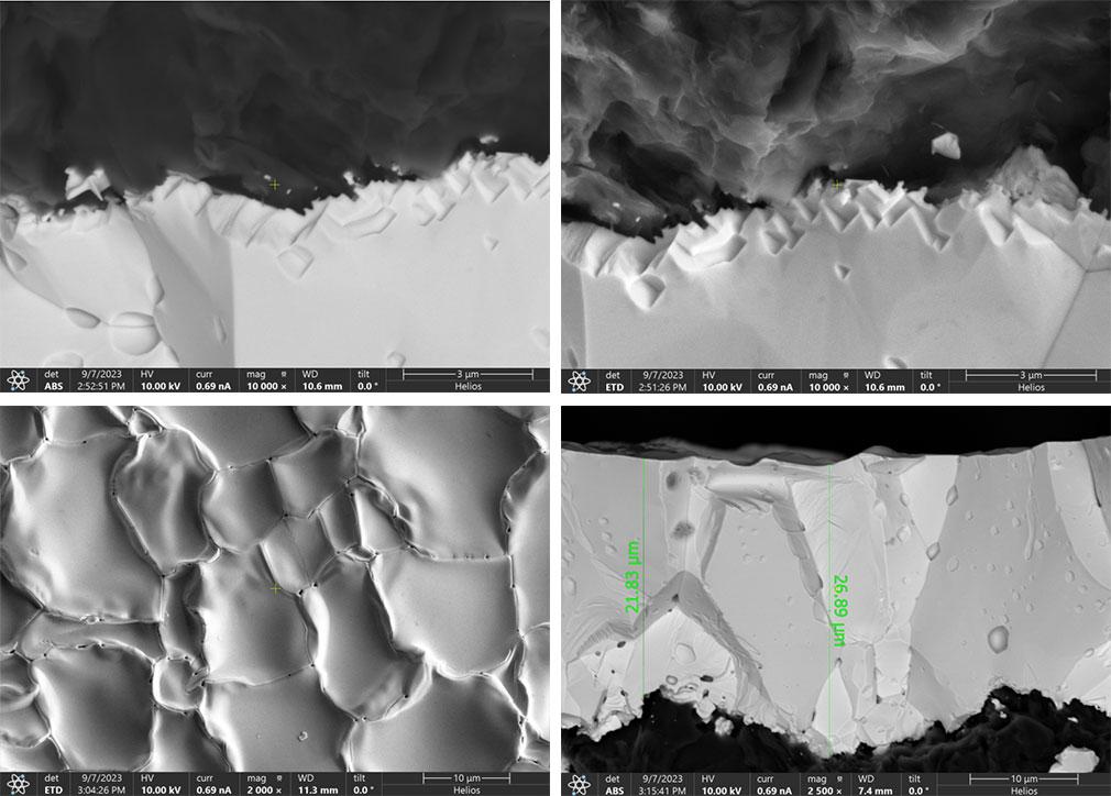
VeTek’s CVD TaC coating features good temperature stability, ultra-high purity, resistance to H₂/NH₃/SiH₄/Si corrosion, strong thermal shock resistance, high adhesion to graphite substrates, and uniform coating coverage. It can be applied to core components such as induction heating susceptors, resistance heating elements, and thermal shielding parts. The company possesses advanced machining capabilities to manufacture graphite, ceramic, or refractory metal substrate components, and provides one-stop in-house processing of SiC or TaC ceramic coatings, as well as coating services for customer-supplied parts.
As the third-generation semiconductor industry accelerates towards larger sizes (8-inch), higher power density, and lower costs, the demands on material performance in manufacturing processes are becoming increasingly stringent. With its extremely high melting point, outstanding chemical inertness, and excellent mechanical properties, CVD TaC coating is becoming the “gold standard” for high-temperature semiconductor processes above 2000°C. From SiC single crystal growth to GaN epitaxy, from MOCVD heaters to wafer carriers, TaC coating provides an indispensable material foundation for semiconductor manufacturing.
VeTek Semiconductor is committed to providing high-quality CVD TaC coating products and customized solutions to global customers through continuous R&D investment and technological iteration. If you require detailed technical data, SEM cross-section analysis, or custom drawing evaluation, please feel free to contact us.
References
[1] Sun, J., Zhang, Q., & Li, X. (2021). Research progress on tantalum carbide coatings on carbon materials. Progress in Materials Science. (Available at ScienceDirect)
[2] Kim, D. Y., et al. (2016). Chemical Vapor Deposition of Tantalum Carbide from TaCl₅-C₃H₆-Ar-H₂ System. Journal of the Korean Ceramic Society, 53(6), 597-603.
[3] Ma, Q., Hu, R., Liu, X., Yang, S., Lu, X., Liu, D., … Gao, P. (2026). Study on the evolution of microstructure and mechanical properties of graphite-based TaC coatings under different harsh conditions. Journal of Alloys and Compounds, 1061. doi:10.1016/j.jallcom.2026.187440
[4] Fan, W., Qu, H., Chang, S. I., et al. (2019). Research on the Impact of TaC Coating on SiC PVT Process Control and Crystal Quality. Joint research data, Dong-Eui University, South Korea.
[5] Meng, J., et al. (2022). Control of the growth quality by optimizing the crucible structure for growth of large-sized SiC single crystal. Journal of Crystal Growth, 600, 126929. doi:10.1016/j.jcrysgro.2022.126929
[6] QYResearch. (2025). Global TaC Coating Market Outlook, In Depth Analysis & Forecast to 2031.
Author: Sera Lee
Tel: 86-15988690905
Email:seralee@veteksemi.com
+86-579-87223657
Wangda Road, Ziyang Street, Wuyi County, Jinhua City, Zhejiang Province, China