




QR Code

Products
Contact Us


Fax
+86-579-87223657

Email

Address
Wangda Road, Ziyang Street, Wuyi County, Jinhua City, Zhejiang Province, China



High-purity materials are essential for semiconductor manufacturing. These processes involve extreme heat and corrosive chemicals. CVD-SiC (Chemical Vapor Deposition Silicon Carbide) provides the necessary stability and strength. It is now a primary choice for advanced equipment parts due to its high purity and density.
1. The Core Principles of CVD Technology
CVD stands for Chemical Vapor Deposition. This process creates solid materials from gas-phase chemical reactions. Manufacturers typically use organic precursors like Methyltrichlorosilane (MTS). Hydrogen acts as the carrier gas for this mixture.
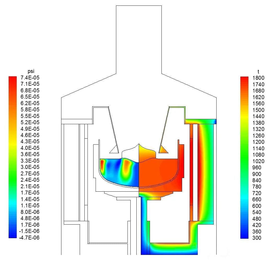
The process takes place in a reaction chamber heated between 1100°C and 1500°C. Gaseous molecules decompose and recombine on the hot substrate surface. Beta-SiC crystals grow layer by layer, atom by atom. This method ensures extremely high chemical purity, often exceeding 99.999%. The resulting material reaches a physical density very close to theoretical limits.
2. SiC Coatings on Graphite Substrates
The semiconductor industry uses graphite for its excellent thermal properties. However, graphite is porous and sheds particles at high temperatures. It also allows gases to permeate easily. Manufacturers solve these issues with the CVD process. They deposit a SiC thin film onto the graphite surface. This layer is usually 100μm to 200μm thick.
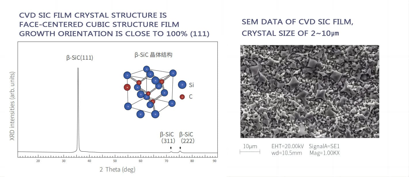
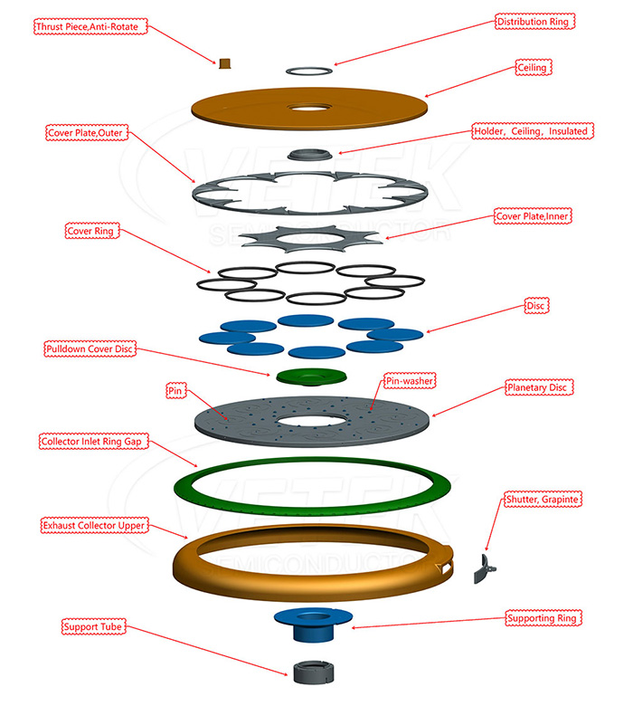
The coating acts as a physical barrier. It prevents graphite particles from contaminating the production environment. It also resists erosion from corrosive gases like ammonia (NH3). A major application is the MOCVD Susceptor. This design combines the thermal uniformity of graphite with the chemical stability of silicon carbide. It keeps the epitaxial layer pure during growth.
3. CVD-Deposited Bulk Materials
Some processes require extreme erosion resistance. Others need to eliminate the substrate entirely. In these cases, Bulk SiC is the best solution. Bulk deposition requires very precise control of reaction parameters. The deposition cycle lasts much longer to grow thick layers. These layers reach several millimeters or even centimeters in thickness.
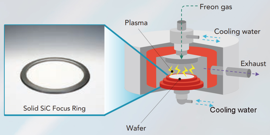
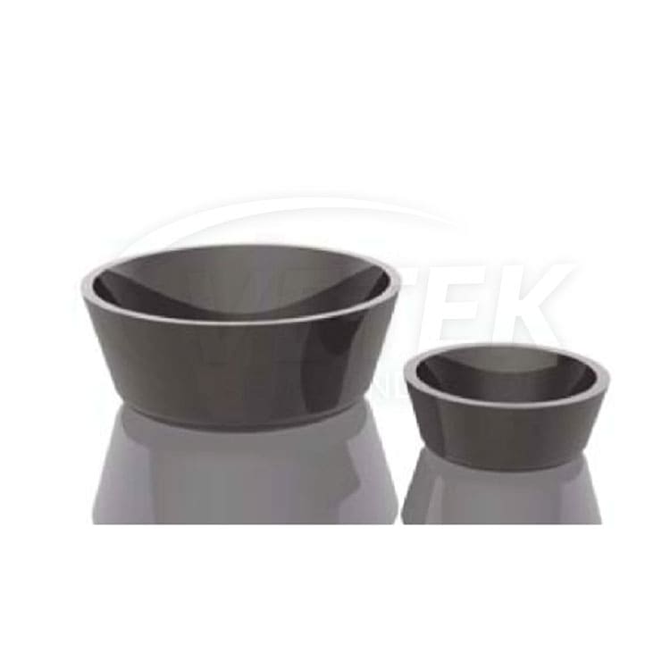
Engineers remove the original substrate to obtain a pure silicon carbide part. These components are critical for Dry Etching equipment. For example, the Focus Ring faces direct exposure to high-energy plasma. Bulk CVD-SiC has very low impurity levels. It offers superior resistance to plasma erosion. This significantly extends the lifespan of the equipment parts.
4. Technical Advantages of the CVD Process
CVD-SiC outperforms traditional press-sintered materials in several ways:
High Purity: Gas-phase precursors allow for deep purification. The material contains no metallic binders. This prevents metal ion contamination during wafer processing.
Dense Microstructure: The atomic stacking creates a non-porous structure. This results in excellent thermal conductivity and mechanical hardness.
Isotropic Properties: CVD-SiC maintains consistent performance in all directions. It resists failure from thermal stress under complex operating conditions.
CVD-SiC technology supports the semiconductor industry through both coatings and bulk structures. At Vetek Semiconductor, we follow the latest advancements in material science. We are dedicated to providing high-quality silicon carbide solutions for the industry.
+86-579-87223657
Wangda Road, Ziyang Street, Wuyi County, Jinhua City, Zhejiang Province, China