


")


QR Code

Products
Contact Us


Fax
+86-579-87223657

E-mail

Address
Wangda Road, Ziyang Street, Wuyi County, Jinhua City, Zhejiang Province, China


How TaC Coating Enhances SiC Crystal Growth in PVT Applications
Silicon carbide (SiC) now underpins much of the progress seen in electric vehicle powertrains, renewable energy converters, and high-frequency power modules. Manufacturing economics and device performance both hinge on enlarging SiC crystal dimensions, boosting batch yields, and suppressing defect populations. Meeting these targets demands more than fine-tuned process recipes. The integrity and longevity of thermal field materials become equally decisive, especially given the aggressive conditions inside Physical Vapor Transport (PVT) furnaces.
Among the surface engineering options for graphite parts, Chemical Vapor Deposition (CVD) of Tantalum Carbide (TaC) has gained measurable traction. This coating does not simply shield the substrate; it actively modifies the surface chemistry and thermal response of components that see the harshest service.
What TaC Coating Does Inside a PVT Furnace?
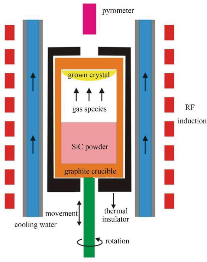
PVT growth proceeds by sublimating SiC feedstock above 2,000°C. The resulting vapor species travel toward a cooler seed crystal, where condensation and recrystallization gradually build the boule. A single run can last hundreds of hours. During this interval, every graphite surface—crucible walls, seed holder, guide rings—faces constant silicon-rich vapor, extreme thermal gradients, and mechanical stress from thermal expansion mismatches.
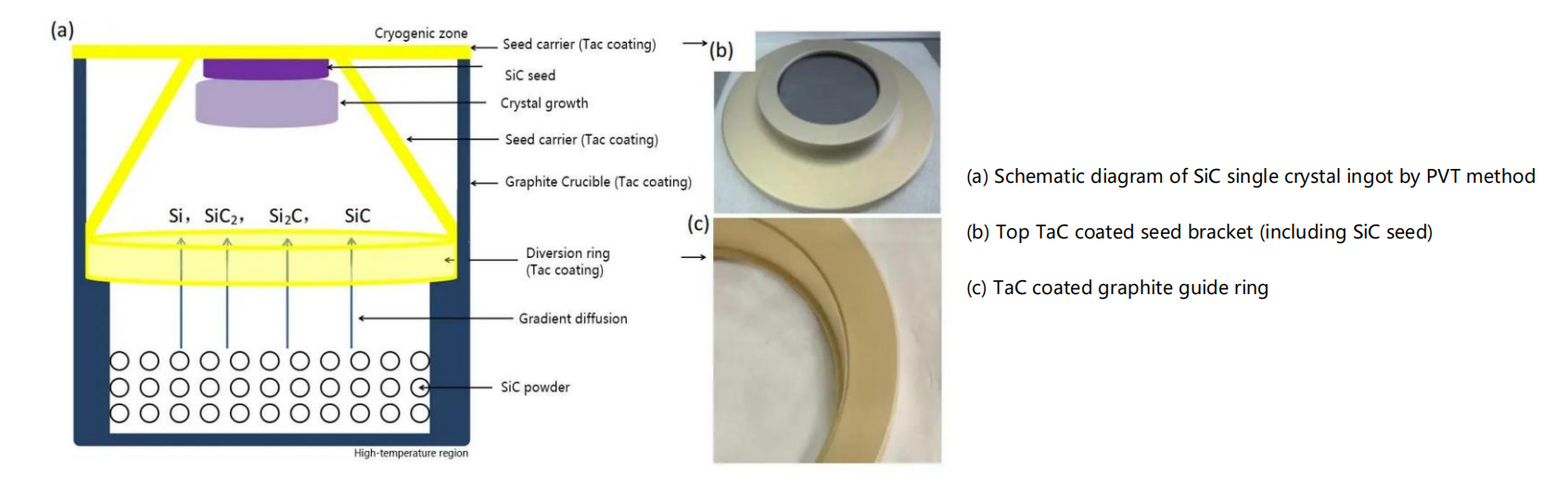
Without protective layers, graphite undergoes two parallel degradation paths. One is physical: surface erosion releases fine carbon particulates into the vapor stream. The other is chemical: silicon vapor reacts with graphite to form volatile SiC or other intermediary species, progressively thinning the component wall. Both pathways introduce carbon clusters or trace metal impurities into the growing crystal, and both shorten the usable life of expensive furnace furniture.
CVD TaC coating interrupts these mechanisms. The coating layer is stoichiometrically controlled, pinhole-free, and adherent to the graphite substrate. It presents a chemically inert face to the high-temperature vapor, so the underlying graphite never directly contacts the reactive environment. This separation fundamentally alters the contamination trajectory.
Observed Improvements in Crystal Quality
Crystal growers often report that TaC-coated components correlate with lower counts of carbon inclusions and micropipe terminations. The explanation lies in the coating's ability to maintain a constant surface condition across multiple runs. Uncoated graphite changes over time—its porosity increases, its emissivity shifts, and its local temperature distribution drifts. These gradual alterations disturb the thermal field symmetry essential for uniform radial growth.
A stable thermal field, by contrast, preserves the axial and radial temperature gradients needed for controlled step-flow growth on the seed surface. With TaC coating, the crucible interior retains its original geometry and thermal emissivity over more growth cycles. The result is a tighter distribution of crystal quality metrics from run to run, which directly raises the fraction of usable wafers per boule.
Extended Component Lifetimes and Operational Cost
The economic case for TaC coating often rests on lifetime extension. Graphite components in uncoated form may need replacement after 10–20 growth runs, depending on the specific temperature profile and run duration. TaC-coated equivalents, in documented furnace operations, routinely achieve 2–3 times that service life before showing measurable weight loss or surface roughening.
This durability stems from the coating's high melting point (exceeding 3,800°C) and its low diffusion coefficient for both carbon and silicon. Even at 2,200°C, interdiffusion across the coating–substrate interface remains negligible. The coating does not spill, flake, or delaminate under thermal cycling, provided the CVD deposition parameters are properly optimized. Longer intervals between component replacements translate to fewer furnace cooldown–heatup cycles, less labor for teardown and reassembly, and lower consumption of high-purity graphite stock.
Purity Specifications That Matter for Semiconductors
For device-grade SiC, metallic impurities at parts-per-million levels can degrade carrier lifetime and breakdown voltage. The coating itself must therefore be semiconductor-compatible. CVD TaC processed from high-purity precursors achieves a documented purity of 99.999841%. This figure is not incidental: it reflects intentional control over precursor gas purification, reactor cleanliness, and post-deposition handling. At this purity level, any metallic species that might diffuse from the coating into the vapor phase remain below analytical detection limits for typical growth durations.
Commonly Coated Graphite Parts
PVT thermal fields typically include five to eight distinct graphite components that can benefit from TaC application:
Crucibles, which contain the SiC source powder and sustain the highest temperatures.
Seed holders, which mount the seed crystal and require precise thermal contact.
Guide rings, which shape the vapor flow path toward the seed.
Crucible rings and spacers, which define the gap between source and seed.
Additional insulation shields or support posts in certain furnace designs.
Coating all or most of these parts creates a consistent surface condition throughout the hot zone, rather than having mixed coated and uncoated surfaces that could introduce localized thermal or chemical asymmetries.
Why CVD Rather Than Other Deposition Methods?
Not all TaC coatings perform identically. Plasma spray or pack cementation routes produce thicker layers but with higher porosity, poorer adhesion, and greater risk of spallation under thermal shock. CVD distinguishes itself by growing the coating atom-by-atom from vapor-phase precursors. This yields fully dense microstructures with grain sizes on the order of a few micrometers and thickness uniformity within ±5 μm across large-area components.
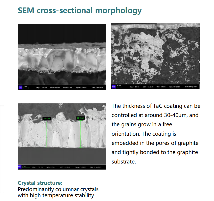
Standard CVD TaC thickness is specified at 30 ± 5 μm for most PVT crucibles and holders. For furnaces running extended cycles or higher peak temperatures, customized thickness up to 40 μm can be applied. Thicker coatings increase the diffusion barrier length but require careful matching to the thermal expansion coefficient of the graphite substrate to avoid interfacial stress—a factor well characterized in CVD process design.
Practical Considerations for Adoption
Facilities transitioning from uncoated to TaC-coated components should anticipate adjustments in temperature control. The coating alters the surface emissivity, which can shift the pyrometer readings or power-to-temperature calibration by 20–50°C. This shift is predictable and repeatable, so a short calibration run suffices to re-establish the correct thermal setpoints. After that initial compensation, the coated system behaves more consistently across runs than its uncoated counterpart, reducing the need for per-run tuning.
Conclusion
PVT-based SiC production places extraordinary demands on graphite thermal field components. CVD TaC coating addresses these demands through four interconnected effects: it suppresses carbon particle release, it blocks silicon attack on the substrate, it preserves thermal field symmetry over extended run sequences, and it prolongs component replacement intervals. These outcomes collectively improve crystal purity, increase usable yield per boule, and reduce the per-wafer cost contribution from consumable parts. As SiC wafer sizes move toward 200 mm and defect density requirements tighten further, the adoption of engineered coatings like TaC is likely to expand from an option to a baseline specification in advanced manufacturing lines.
+86-579-87223657
Wangda Road, Ziyang Street, Wuyi County, Jinhua City, Zhejiang Province, China