


QR Code

Products
Contact Us


Fax
+86-579-87223657

E-mail

Address
Wangda Road, Ziyang Street, Wuyi County, Jinhua City, Zhejiang Province, China


In the world of Silicon Carbide (SiC) semiconductors, most of the spotlight shines on 8-inch epitaxial reactors or the intricacies of wafer polishing. However, if we trace the supply chain back to the very beginning—inside the Physical Vapor Transport (PVT) furnace—a fundamental "material revolution" is quietly taking place.
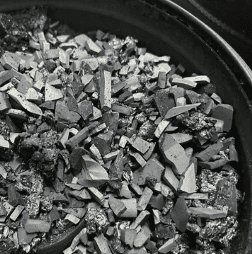
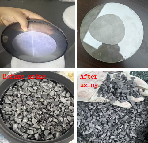
For years, synthesized SiC powder has been the industry workhorse. But as the demand for high yields and thicker crystal boules becomes almost obsessive, the physical limitations of traditional powder are reaching a breaking point. This is why 7N Bulk CVD SiC raw material has moved from the periphery to the center of technical discussions.
What Does an Extra Two "Nines" Actually Mean?
In semiconductor materials, the leap from 5N (99.999%) to 7N (99.99999%) might look like a minor statistical tweak, but at the atomic level, it is a total game-changer.
Traditional powders often struggle with trace metallic impurities introduced during synthesis. In contrast, bulk material produced via Chemical Vapor Deposition (CVD) can drive impurity concentrations down to the parts-per-billion (ppb) level. For those growing High-Purity Semi-Insulating (HPSI) crystals, this level of purity isn't just a vanity metric—it’s a necessity. The ultra-low Nitrogen (N) content is the primary factor that dictates whether a substrate can maintain the high resistivity required for demanding RF applications.
Solving "Carbon Dust" Pollution: A Physical Fix for Crystal Defects
Anyone who has spent time around a crystal growth furnace knows that "carbon inclusions" are the ultimate nightmare.
When using powder as a source, temperatures exceeding 2000°C often cause the fine particles to graphitize or collapse. These tiny, unanchored "carbon dust" particles can be carried by gas currents and land directly on the crystal growth interface, creating dislocations or inclusions that effectively scrap the entire wafer.
CVD-SiC bulk material operates differently. Its density is nearly theoretical, meaning it behaves more like a melting ice block than a pile of sand. It sublimes uniformly from the surface, physically cutting off the source of dust. This "clean growth" environment provides the foundational stability needed to push the yields of large-diameter 8-inch crystals.
Kinetics: Breaking the 0.8 mm/h Speed Limit
Growth rate has long been the "Achilles' heel" of SiC productivity. In traditional setups, rates usually hover between 0.3 - 0.8mm/h, making growth cycles last a week or more.
Why can switching to bulk material push these rates to 1.46mm/h? It comes down to the mass transfer efficiency within the thermal field:
1. Optimized Packing Density: The structure of bulk material in the crucible helps maintain a more stable and steeper temperature gradient. Basic thermodynamics tells us that a larger gradient provides a stronger driving force for gas phase transport.
2. Stoichiometric Balance: Bulk material sublimes more predictably, smoothing out the common headache of being "Si-rich" at the start of growth and "C-rich" toward the end.
This inherent stability allows crystals to grow thicker and faster without the usual trade-off in structural quality.
Conclusion: An Inevitability for the 8-Inch Era
As the industry pivots fully toward 8-inch production, the margin for error has vanished. The transition to high-purity bulk materials is no longer just an "experimental upgrade"—it is the logical evolution for manufacturers pursuing high-yield, high-quality results.
Moving from powder to bulk is more than just a change in shape; it is a fundamental reconstruction of the PVT process from the bottom up.
+86-579-87223657
Wangda Road, Ziyang Street, Wuyi County, Jinhua City, Zhejiang Province, China