News

PZT Piezoelectric Wafers: High-Performance Solutions for Next-Gen MEMS

2026-03-20 0 Leave me a message

In the era of rapid MEMS (Micro-Electromechanical Systems) evolution, selecting the right piezoelectric material is a make-or-break decision for device performance. PZT (Lead Zirconate Titanate) thin-film wafers have emerged as the premier choice over alternatives like AlN (Aluminum Nitride), offering superior electromechanical coupling for cutting-edge sensors and actuators.

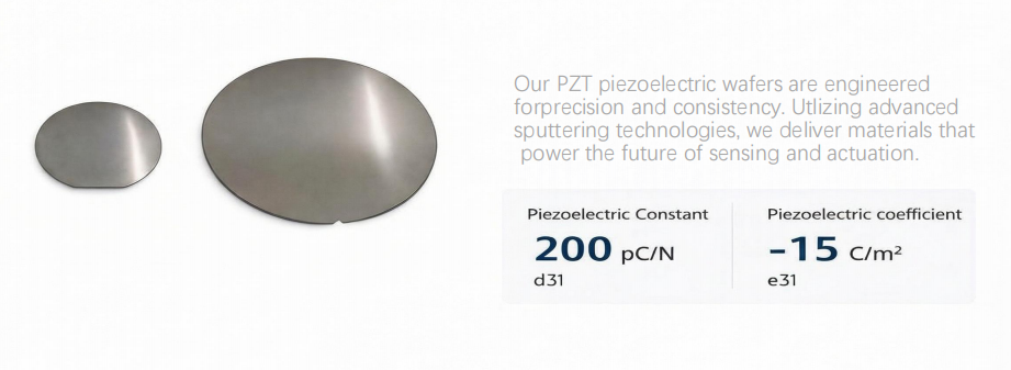
Vetek Semiconductor provides industry-leading PZT-on-Si/SOI wafers. Leveraging advanced thin-film deposition, we deliver exceptional film uniformity and crystalline quality, specifically engineered to overcome common industry hurdles like film fatigue and performance degradation.


Core Architecture: The Synergy of Pt and PZT

The integrity of the multi-layer stack is fundamental to ferroelectric performance. Our wafers utilize a precision-engineered stack of metallic electrodes and ceramic thin films:

  • The PZT Piezoelectric Core: Our process focuses on rigorous crystal orientation control. According to Muralt (2000), PZT with a (100) or (001) preferred orientation yields a significantly higher longitudinal piezoelectric constant. Vetek’s optimized deposition ensures a strong (100) orientation, enabling massive energy output even at micron-level thicknesses.
  • The Critical Pt Electrode Layer: Platinum (Pt) serves as both the electrical conduit and the growth template for PZT. Renowned for its high conductivity and thermal stability in oxygen-rich environments, Pt is the industry gold standard for bottom electrodes (Takahashi et al., 1994). We maintain ultra-low surface roughness (Ra <= 1.0 nm) to provide an ideal interface for PZT nucleation.
  • Integrated Buffer Layers: To suppress elemental diffusion between the PZT and the Silicon substrate, we incorporate a precision Buffer Layer system. These layers act as a physical barrier and stress-buffer, preventing film delamination and ensuring the mechanical reliability of the entire wafer during complex MEMS etching.


Target Applications: Where is PZT Used?

High-performance PZT wafers are essential for applications requiring precise mechanical-to-electrical sensing or electrical-to-mechanical actuation:

  • Consumer Electronics (PMUT): Target Clients include smartphone module manufacturers and biometric security firms. Use Case: PZT films generate high-frequency ultrasonic waves for under-display fingerprint sensing. Compared to legacy solutions, PZT-based PMUTs offer deeper penetration and higher resolution (Akbari et al., 2016), enabling secure 3D biometric authentication.
  • Telecmmunications (RF MEMS): Target Clients include RF front-end chip designers and 5G/6G infrastructure providers. Use Case: Utilizing PZT’s high electromechanical coupling coefficient to create tunable filters. This minimizes signal loss and expands bandwidth, critical for managing spectrum congestion in 5G networks.
  • Industrial Printing: Target Clients include industrial inkjet printer manufacturers and flexible display (OLED) makers. Use Case: PZT wafers are micro-machined into ultra-fast actuators. By deforming the ink chamber instantaneously, they achieve pico-liter precision fluid dispensing, a cornerstone for OLED manufacturing and high-res 3D printing.
  • Healthcare: Target Clients include medical device R&D and handheld ultrasound startups. Use Case: Driving Intravascular Ultrasound (IVUS) probes for internal imaging. It also serves as the heart of high-efficiency, silent medical nebulizers for targeted drug delivery.
  • Automotive: Target Clients include autonomous driving solution providers and smart cockpit HMI developers. Use Case: Extending the detection range of automotive ultrasonic sensors. Additionally, it provides Haptic Feedback in touchscreens, simulating the tactile feel of physical buttons.

Beyond MEMS devices, the same precision manufacturing principles enable high-reliability visual solutions like Transparent LED Display , which demand consistent quality across thousands of modules.


Why Choose Vetek Semiconductor?

  • Superior Parameters: Piezoelectric constant d31 typically reaches 200 pC/N, with an e31 coefficient stable at -15 C/m2.
  • Versatile Substrates: Available in 6-inch and 8-inch formats, including high-resistivity SOI substrates (> 5000 ohm/cm).
  • Bespoke Customization: We support Customer Supplied Wafers (Foundry Service) and can customize the thickness ratio of PZT and Pt layers to match your specific resonance frequency requirements.


Author: Sera Lee


Academic References:

[1] Muralt, P. (2000). "PZT thin films for microsensors and actuators: problems and progress." Journal of Micromechanics and Microengineering.

[2] Trolier-McKinstry, S., et al. (2018). "Piezoelectric Thin Films for MEMS." Annual Review of Materials Research.

[3] Akbari, M., et al. (2016). "Piezoelectric Micromachined Ultrasonic Transducers (pMUTs) for Medical Imaging." In Piezoelectric MEMS Resonators.

Related News
Leave me a message
X
We use cookies to offer you a better browsing experience, analyze site traffic and personalize content. By using this site, you agree to our use of cookies.Privacy Policy
RejectAccept