


QR Code

Products
Contact Us


Fax
+86-579-87223657

E-mail

Address
Wangda Road, Ziyang Street, Wuyi County, Jinhua City, Zhejiang Province, China


With the global energy transition, the AI revolution, and the wave of new-generation information technologies, silicon carbide (SiC) has rapidly advanced from being a "potential material" to a "strategic foundational material" due to its exceptional physical properties. Its applications are expanding at an unprecedented pace, placing nearly extreme demands on the quality and consistency of substrate materials. This has made addressing critical defects such as "carbon encapsulation" more urgent and necessary than ever before.
Frontier Applications Driving SiC Substrates
1.AI Hardware Ecosystem and the Limits of Miniaturization:
The next generation of AI glasses (AR/VR devices) strives for an unparalleled sense of immersion and real-time interaction. This means that their internal core processors (such as dedicated AI inference chips) must process vast amounts of data and handle significant heat dissipation within extremely limited miniaturized space. Silicon-based chips face physical limitations in this scenario.
AR/VR optical waveguides require a high refractive index to reduce device volume, broad-band transmission to support full-color displays, high thermal conductivity to manage heat dissipation from high-power light sources, and high hardness and stability to ensure durability. They must also be compatible with mature micro/nano-optical processing technologies for large-scale manufacturing.
Role of SiC: GaN-on-SiC RF/power modules made from SiC substrates are key to resolving this contradiction. They can drive miniature displays and sensor systems with higher efficiency and, with thermal conductivity several times higher than silicon, quickly dissipate the massive heat generated by chips, ensuring stable operation in a slim form factor.
Single-crystal silicon carbide (SiC) has a refractive index of about 2.6 in the visible light spectrum, with excellent transparency, making it suitable for high-integrated optical waveguide designs. Based on its high refractive index properties, a single-layer SiC diffraction waveguide can theoretically achieve a field of view (FOV) of around 70° and effectively suppress rainbow patterns. Moreover, SiC has extremely high thermal conductivity (about 4.9 W/cm·K), allowing it to rapidly dissipate heat from optical and mechanical sources, preventing optical performance degradation due to temperature rise. Additionally, SiC's high hardness and wear resistance significantly enhance the structural stability and long-term durability of the waveguide lenses. SiC wafers can be used for micro/nano processing (such as etching and coating), facilitating the integration of micro-optical structures.
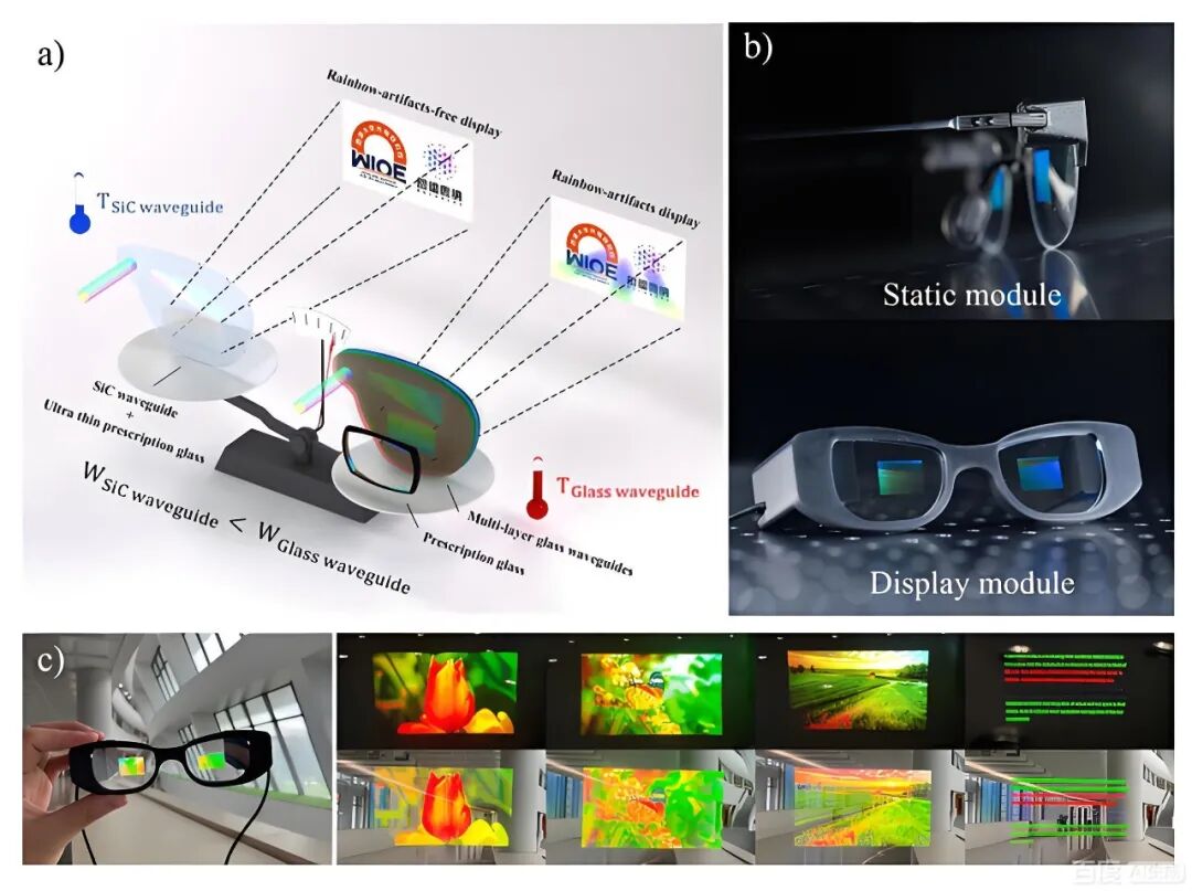
The hazards of "carbon encapsulation": If the SiC substrate contains a "carbon encapsulation" defect, it becomes a localized "thermal insulator" and "electrical fault point." Not only does it severely obstruct heat flow, leading to local overheating of the chip and performance degradation, but it may also cause micro-discharges or leakage currents, potentially leading to display anomalies, calculation errors, or even hardware failure in AI glasses under long-term high-load conditions. Therefore, a defect-free SiC substrate is the physical foundation for achieving reliable, high-performance wearable AI hardware.
The hazards of "carbon encapsulation": If the SiC substrate contains a "carbon encapsulation" defect, it will reduce the transmission of visible light through the material, and may also lead to localized overheating of the waveguide, performance degradation, and a decrease or abnormality in display brightness.
2.The Revolution in Advanced Computing Packaging:
In the AI computing power race led by NVIDIA, advanced packaging technologies like CoWoS (Chip-on-Wafer-on-Substrate) have become central to integrating CPUs, GPUs, and HBM memory, enabling exponential growth in computing power. In this complex heterogeneous integration system, the interposer plays a critical role as the backbone for high-speed interconnects and thermal management.
Role of SiC: Compared to silicon and glass, SiC is considered the ideal material for the next-generation high-performance interposer due to its extremely high thermal conductivity, a coefficient of thermal expansion that matches better with chips, and excellent electrical insulation properties. SiC interposers can more efficiently dissipate concentrated heat from multiple computing cores and ensure the integrity of high-speed signal transmission.
The hazards of "carbon encapsulation": Beneath nanometer-level interconnects, a micron-level "carbon encapsulation" defect is like a "time bomb." It can distort local thermal and stress fields, leading to thermomechanical fatigue and cracking in the interconnect metal layers, causing signal delays, crosstalk, or complete failure. In AI acceleration cards worth hundreds of thousands of RMB, system failures caused by underlying material defects are unacceptable. Ensuring the absolute purity and structural perfection of the SiC interposer is the cornerstone of maintaining the reliability of the entire complex computing system.
Conclusion: Transition from "acceptable" to "perfect and flawless." In the past, silicon carbide was mainly used in industrial and automotive fields, where some tolerance for defects existed. However, when it comes to the miniaturization world of AI glasses and ultra-high-value, ultra-complex systems like NVIDIA's CoWoS, the tolerance for material defects has dropped to zero. Every "carbon encapsulation" defect directly threatens the performance limits, reliability, and commercial success of the end product. Therefore, overcoming substrate defects like "carbon encapsulation" is no longer just an academic or process improvement issue but a critical material battle that supports the next-generation artificial intelligence, advanced computing, and consumer electronics revolution.
Where Does Carbon Wrapping Come From
Rost et al. proposed the "concentration model," suggesting that changes in the ratio of substances in the gas phase are the main cause of carbon encapsulation. Li et al. found that seed graphitization can induce carbon encapsulation before growth begins. Due to the escape of silicon-rich atmosphere from the crucible and the active interaction between the silicon atmosphere and the graphite crucible and other graphite elements, the graphitization of the silicon carbide source is inevitable. Therefore, the relatively low Si partial pressure in the growth chamber may be the main cause of carbon encapsulation. However, Avrov et al. argued that carbon encapsulation is not caused by silicon deficiency. Thus, the strong corrosion of graphite elements due to excess silicon might be the main cause of carbon inclusions. Direct experimental evidence in this paper shows that fine carbon particles on the source surface can be driven into the growth front of silicon carbide single crystals, forming carbon encapsulations. This result indicates that the generation of fine carbon particles in the growth chamber is the primary cause of carbon encapsulation. The appearance of carbon encapsulation in silicon carbide single crystals is not due to the low partial pressure of Si in the growth chamber, but rather the formation of weakly connected carbon particles due to the graphitization of the silicon carbide source and corrosion of graphite elements.
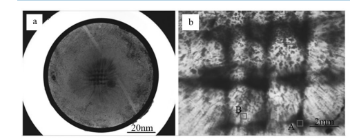
The distribution of inclusions seems to closely resemble the pattern of the graphite plates on the source surface. The inclusion-free zones in the single crystal wafers are circular, with a diameter of about 3mm, which perfectly corresponds to the diameter of the perforated circular holes. This suggests that carbon encapsulation originates from the raw material area, meaning the graphitization of the raw material causes the carbon encapsulation defect.
Silicon carbide crystal growth typically requires 100-150 hours. As the growth progresses, the graphitization of the raw material becomes more severe. Under the demand for growing thick crystals, addressing the graphitization of the raw material becomes a key issue.
Carbon Wrapping Solution
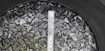
1.The Sublimation Theory of Raw Materials in PVT
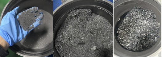
As seen in the above diagram, increasing the raw material particle size helps suppress the preferential volatilization of the Si component in the raw material, making the gas phase composition during the entire growth process more stable and addressing the graphitization issue of the raw material. Large particle CVD materials, especially raw materials larger than 8mm in size, are expected to completely solve the graphitization problem, thereby eliminating the carbon encapsulation defect in the substrate.
Conclusion And Prospect
The large-particle, high-purity, stoichiometric SiC raw material synthesized by the CVD method, with its inherent low surface area to volume ratio, provides a highly stable and controllable sublimation source for SiC single crystal growth using the PVT method. This is not only a change in the form of the raw material but also fundamentally reshapes and optimizes the thermodynamic and kinetic environment of the PVT method.
The application advantages are directly translated into:
+86-579-87223657
Wangda Road, Ziyang Street, Wuyi County, Jinhua City, Zhejiang Province, China