


QR Code

Products
Contact Us


Fax
+86-579-87223657

E-mail

Address
Wangda Road, Ziyang Street, Wuyi County, Jinhua City, Zhejiang Province, China


In advanced semiconductor manufacturing, the industry has squeezed every last drop of performance out of "Graphite + SiC Coating" setups. It worked for years, but as we push into 3nm and beyond, that old interface between the substrate and the shield is becoming a massive headache. The CTE mismatch isn't just a theoretical problem anymore—it’s a yield killer causing micro-cracks that just won't go away.
That’s why the shift toward monolithic CVD Solid SiC is more than just a trend; it's a mechanical necessity. We're moving from a simple surface treatment to a full-on structural material grown from the ground up.
![]()
1. Core Process: Synthesizing High-Purity CVD Solid SiC
Fabricating a pure CVD Solid SiC ingot is a different beast entirely compared to standard deposition. It starts with Methyltrichlorosilane (MTS), but the magic happens in the stability of the reaction over time.
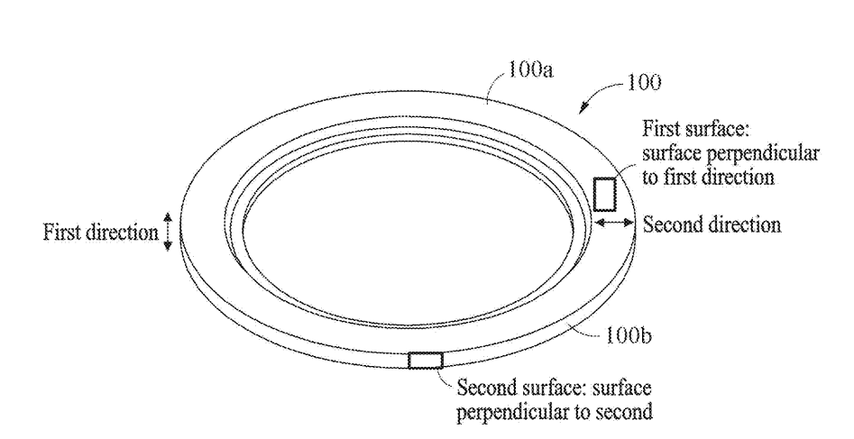
Structural Diagram: As illustrated in Figure, fabricating CVD Solid SiC components requires absolute control over geometric orientation. By optimizing deposition parameters, we ensure that the material possesses highly consistent physical properties across all dimensions (First and Second directions). This structural stability ensures that the parts maintain exceptional flatness and surface perpendicularity after machining, perfectly meeting the rigorous tolerances of 8-inch and 12-inch high-volume manufacturing lines.
2. Why Choose CVD Solid SiC?
Compared to Sintered SiC or traditional coatings, CVD Solid SiC offers unparalleled advantages:
3. Key Application Fields
High-purity CVD Solid SiC materials are essential for high-stress environments:
![]()
4.Conclusion
While the CVD Solid SiC process involves a higher initial manufacturing threshold, the comprehensive return on investment (ROI) is clear. By significantly extending the service life of critical consumables and reducing wafer scrap rates, CVD Solid SiC empowers fabs to achieve long-term cost reduction and efficiency gains.
+86-579-87223657
Wangda Road, Ziyang Street, Wuyi County, Jinhua City, Zhejiang Province, China