


QR Code

Products
Contact Us


Fax
+86-579-87223657

Email

Address
Wangda Road, Ziyang Street, Wuyi County, Jinhua City, Zhejiang Province, China


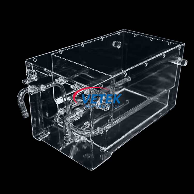
The AMAT Cover Top Quartz 8 inch PCII (Part No. 0200-00218) is a high-purity quartz component designed for use in 200mm (8-inch) PVD process chambers, specifically compatible with Applied Materials Endura® platform (PCII chamber).
Manufactured from ultra-high purity fused quartz, this component plays a critical role in maintaining a clean and stable deposition environment by minimizing contamination and ensuring consistent plasma behavior.
At Vetek Semiconductor, we provide precision-engineered quartz parts with strict material control and dimensional accuracy, offering reliable alternatives for semiconductor fabs and equipment service providers.
Key Specifications:
|
Product Name |
Cover Top Quartz |
|
Part Number |
0200-00218 |
|
Wafer Size |
8 inch (200mm) |
|
Material |
High-Purity Fused Quartz |
|
Application |
PVD (Physical Vapor Deposition) |
|
Compatible Equipment |
Applied Materials Endura® (PCII Chamber) |
This quartz cover is specifically designed for PVD sputtering processes, widely used in semiconductor manufacturing for metal thin film deposition such as aluminum (Al), titanium (Ti), and copper (Cu).
Chamber Position
The component is installed in the upper section of the PVD chamber, commonly referred to as the top cover region, where it is exposed to:
● Plasma discharge zones
● Process gas flow paths
● Metal particle deposition environments
Functional Role in the Chamber
Within the chamber structure, the Cover Top Quartz serves as a non-metallic protective barrier and insulating element, positioned above the wafer and near the target region.
Its placement is critical for:
● Shielding sensitive chamber components from metal deposition
● Maintaining electrical insulation in RF plasma environments
● Supporting stable and repeatable process conditions
1) Contamination Control
During PVD processes, sputtered metal atoms tend to deposit not only on wafers but also on internal chamber surfaces.
This quartz cover:
● Acts as a sacrificial protective layer
● Prevents metal buildup on critical chamber structures
● Reduces particle generation and cross-contamination
Result: Improved wafer yield and process cleanliness
2) Plasma Stability & Electrical Insulation
Thanks to its excellent dielectric properties, high-purity quartz ensures:
● Stable RF field distribution
● Reduced risk of electrical interference
● Consistent plasma density across process cycles
Result: Enhanced film uniformity and repeatability
3) Superior Material Purity
Vetek Semiconductor utilizes ultra-high purity quartz materials to minimize impurity introduction.
● Low metallic contamination
● Minimal outgassing under vacuum conditions
● Suitable for advanced semiconductor nodes
Result: Meets stringent fab-level cleanliness standards
4) Excellent Plasma & Thermal Resistance
The component is engineered to withstand:
● Plasma erosion and ion bombardment
● Repeated thermal cycling
Result: Longer service life and reduced maintenance frequency
5) Cost-Effective Consumable Design
As a replaceable chamber consumable, this part:
● Protects expensive chamber hardware
● Simplifies maintenance cycles
● Lowers total cost of ownership (TCO)
At Vetek Semiconductor, we combine materials science expertise with semiconductor process understanding to deliver high-performance quartz components.
Our Advantages:
● Precision machining with tight tolerances
● Strict raw material selection and traceability
● Proven compatibility with AMAT Endura platforms
● Stable supply for global semiconductor customers
● Engineering support for customization and optimization

Address
Wangda Road, Ziyang Street, Wuyi County, Jinhua City, Zhejiang Province, China
Tel
+86-579-87223657
Wangda Road, Ziyang Street, Wuyi County, Jinhua City, Zhejiang Province, China