
Products

Support Service

View as  
 
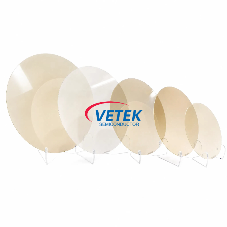
Aluminum Nitride (AlN) Wafers

Aluminum Nitride (AlN) Wafers

VeTek Semiconductor supplies high-quality Aluminum Nitride (AlN) single-crystal wafers and substrates for next-generation ultra-wide-bandgap semiconductor devices. With an ultra-wide bandgap of approximately 6.2 eV, outstanding thermal conductivity, exceptional electrical insulation, and excellent lattice and thermal-expansion match with GaN, AlN wafers are ideal for high-power RF devices, high-voltage power electronics, and deep-ultraviolet (DUV) optoelectronics.
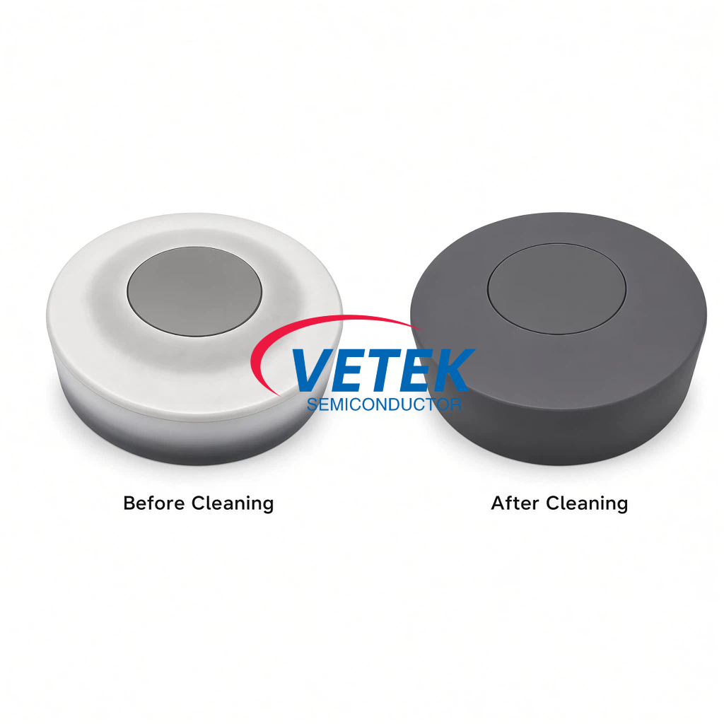
CVD SiC Coating Graphite Parts Cleaning Service

CVD SiC Coating Graphite Parts Cleaning Service

VETEK Professional Cleaning Service for CVD SiC Coated Graphite Parts is a specialized technical service designed for Aixtron / Veeco MOCVD equipment susceptors and graphite components used in GaN / AlN / AlGaN epitaxial processes. Our proprietary cleaning process thoroughly eliminates surface memory effect, restores stable gas flow in the reactor, and strictly protects the 100 µm CVD SiC coating with absolute zero thickness loss and zero metal residue.
PZT Piezoelectric Wafers (PZT on Si/SOI)

PZT Piezoelectric Wafers (PZT on Si/SOI)

As the demand for high-sensitivity and low-power MEMS transducers grows with the expansion of 5G communications, precision medical devices, and smart wearables, our PZT on Si/SOI wafers provide a critical material solution. Utilizing advanced thin-film deposition processes such as Sol-gel or sputtering, we achieve exceptional consistency and superior piezoelectric performance on silicon substrates. These wafers serve as the fundamental core for electromechanical energy conversion.
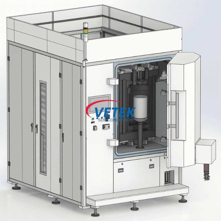
Large sized resistance heating SiC crystal growth furnace

Large sized resistance heating SiC crystal growth furnace

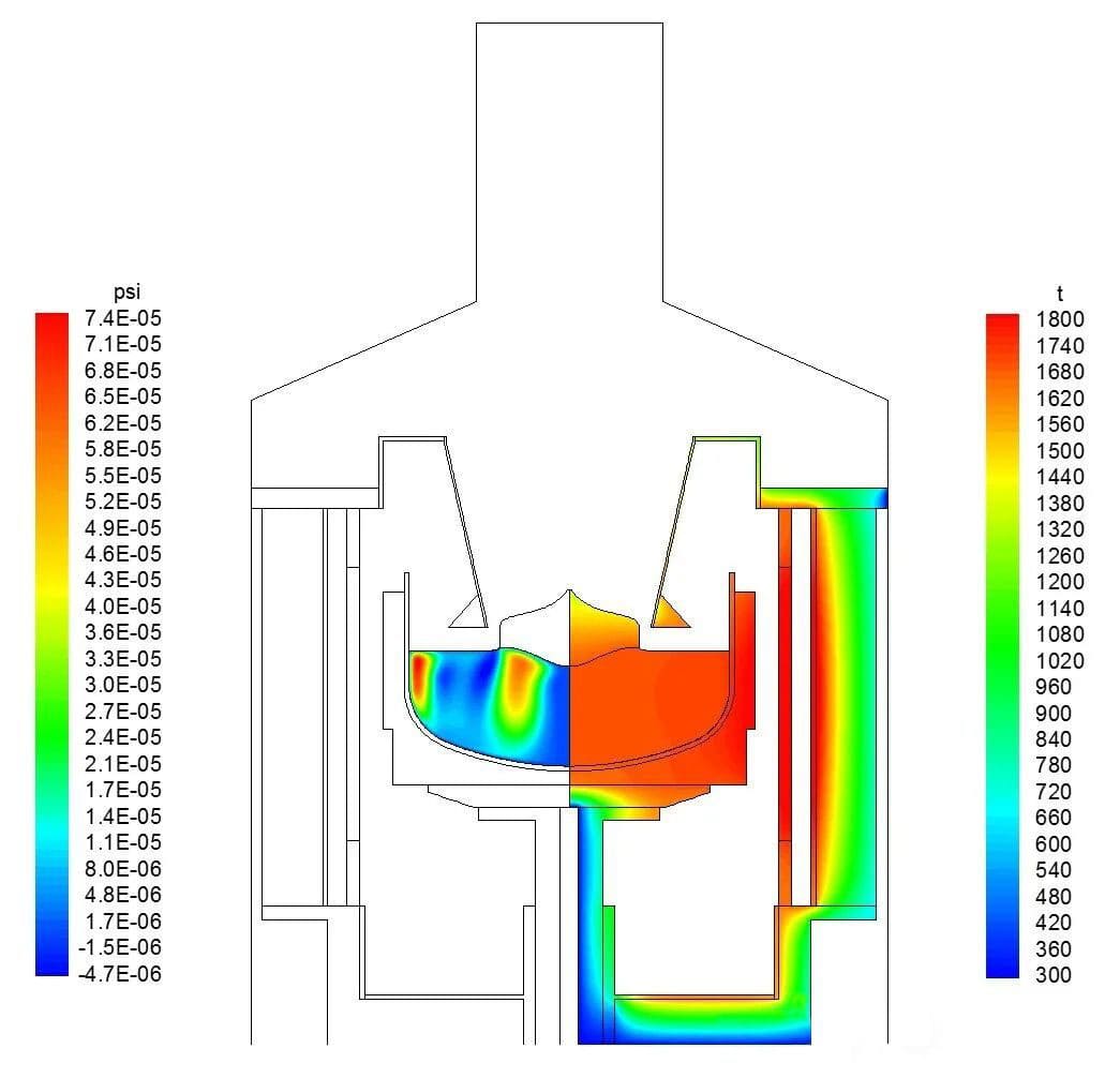
Silicon carbide crystal growth is a core process in the manufacturing of high-performance semiconductor devices. The stability, precision, and compatibility of crystal growth equipment directly determine the quality and yield of silicon carbide ingots. Based on the characteristics of Physical Vapor Transport (PVT) technology, Veteksemi has developed a resistance heating furnace for silicon carbide crystal growth, enabling stable growth of 6-inch, 8-inch, and 12-inch silicon carbide crystals with full compatibility with conductive, semi-insulating, and N-type material systems. Through precise control of temperature, pressure, and power, it effectively reduces crystal defects such as EPD (Etch Pit Density) and BPD (Basal Plane Dislocation), while featuring low energy consumption and a compact design to meet the high standards of industrial large-scale production.
CMP Polishing Slurry

CMP Polishing Slurry

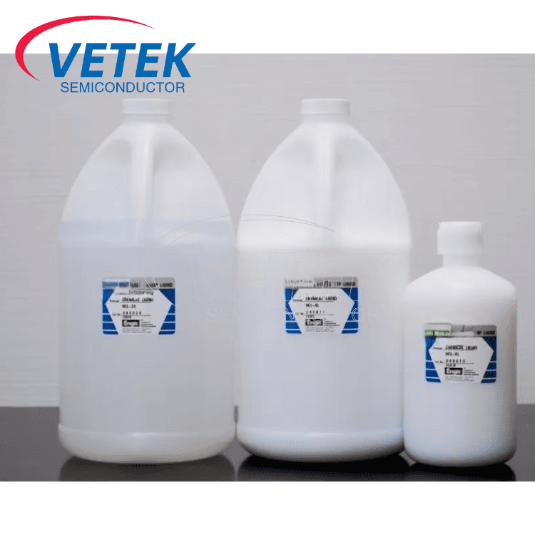
CMP polishing slurry (Chemical Mechanical Polishing Slurry) is a high-performance material used in semiconductor manufacturing and precision material processing. Its core function is to achieve fine flatness and polishing of the material surface under the synergistic effect of chemical corrosion and mechanical grinding to meet the flatness and surface quality requirements at the nano level. Looking forward to your further consultation.
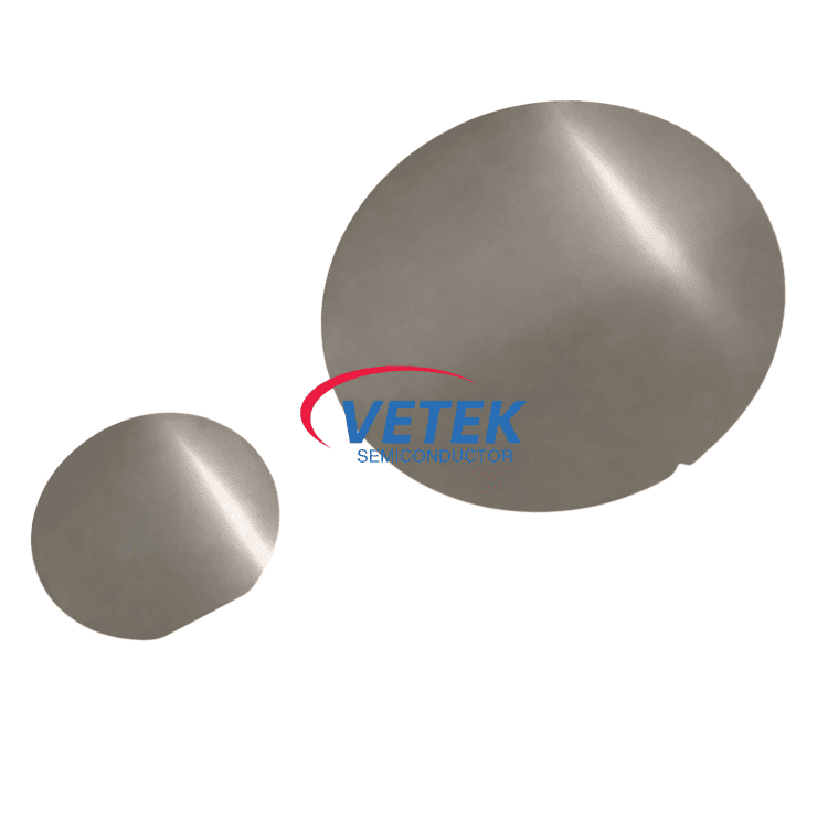
CVD SiC coating Dummy wafer

CVD SiC coating Dummy wafer

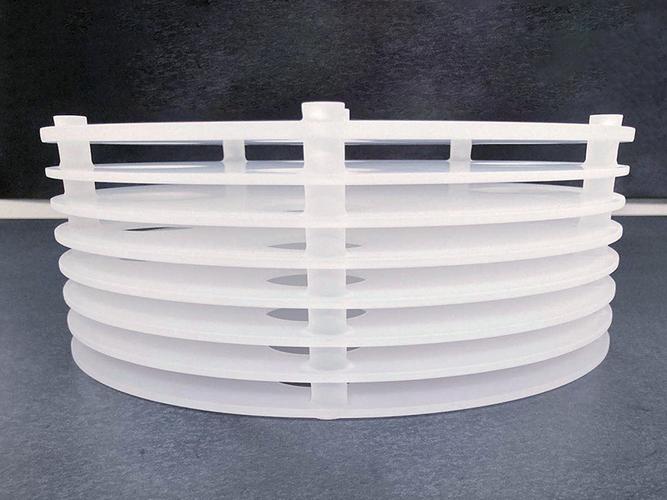
As a leading Chinese sic wafer manufacturers and suppliers, VeTek Semiconductor CVD SiC coating Dummy wafer is a specialized tool in semiconductor manufacturing, mainly used for the purpose of silicon wafer testing and wafer testing process. Your further inquiries are welcome.
As a professional Support Service manufacturer and supplier in China, we have our own factory. Whether you need customized services to meet the specific needs of your region or want to buy advanced and durable Support Service made in China, you can leave us a message.
X
We use cookies to offer you a better browsing experience, analyze site traffic and personalize content. By using this site, you agree to our use of cookies.Privacy Policy