



QR Code

Products
Contact Us


Fax
+86-579-87223657

Email

Address
Wangda Road, Ziyang Street, Wuyi County, Jinhua City, Zhejiang Province, China


• Ultra-wide bandgap ≈ 6.2 eV — highest among mainstream semiconductor materials
• High thermal conductivity ≈ 320 W/m·K for efficient heat dissipation
• Excellent electrical insulation (>10¹³ Ω·cm) and high breakdown field (12–15 MV/cm)
• Good lattice and thermal-expansion match with GaN — ideal for GaN-on-AlN heterostructures
• Low dislocation density options with tight HR-XRD rocking-curve control
• Al-face CMP (Ra ≤ 0.5 nm) and N-face MP for epi-ready surfaces
• Multiple sizes and quality grades (P / R / D) to match production and research requirements
• High-power RF devices for radar and 6G communications
• High-voltage power electronics for grid, data centers, and electric vehicles
• Deep-ultraviolet (UVC) LEDs and laser diodes
• GaN-on-AlN epitaxial growth and advanced heterostructure devices
• High-temperature, high-frequency, and harsh-environment semiconductor components
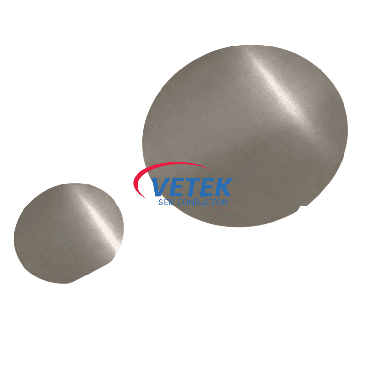
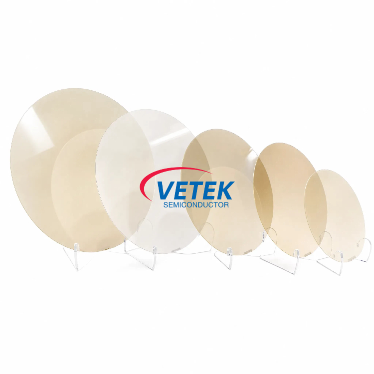
VeTek offers AlN wafers in the following standard formats. Custom sizes and specifications can be discussed upon request.
• 10 × 10 mm square substrates
• 1-inch (25.4 mm) wafers
• 2-inch (50.8 mm) wafers
Quality grades: P-grade (Product), R-grade (Research), D-grade (Experimental), differentiated mainly by HR-XRD rocking-curve FWHM and overall crystal quality.
Common parameters across sizes (typical values; grade-dependent where noted):
|
Parameter |
P-Grade |
R-Grade |
D-Grade |
|
Orientation |
(0001) ± 0.5° |
||
|
Thickness |
450 μm ± 25 μm |
||
|
HR-XRD FWHM (002) |
≤ 100 arcsec |
≤ 200 arcsec |
≤ 300 arcsec |
|
HR-XRD FWHM (102) |
≤ 80 arcsec |
≤ 150 arcsec |
≤ 250 arcsec |
|
Surface Polish |
Al-face CMP, N-face MP |
||
|
Surface Roughness Ra |
Al ≤ 0.5 nm; N ≤ 1.2 μm |
||
|
Scratches / Chipping (naked eye) |
None |
||
|
Edge Exclusion |
1 mm |
||
|
Packaging |
Single-wafer box |
||
Size-specific geometric tolerances:
• 10×10 mm: Side length 10 mm ± 0.5 mm; TTV ≤ 15 μm; Bow ≤ 15 μm
• 1-inch: Diameter 25.4 mm ± 0.5 mm; Usable area ≥ 90%; TTV ≤ 20 μm; Bow ≤ 20 μm; Primary flat (10-10) ± 5°, length 8 mm ± 1 mm
• 2-inch: Diameter 50.8 mm ± 0.5 mm; Usable area ≥ 90%; TTV ≤ 30 μm; Bow ≤ 30 μm; Primary flat length 16 mm ± 2 mm
As a specialized supplier of advanced semiconductor materials and components, VeTek Semiconductor provides:
• High-quality AlN single-crystal wafers with controlled crystal quality and epi-ready surfaces
• Multiple size and grade options to support both device production and research programs
• Complementary wafer and substrate solutions under the VeTek semiconductor materials portfolio
• Technical support for material selection and process matching
Our AlN wafers help customers accelerate development of high-power RF, high-voltage power, and deep-UV optoelectronic devices that demand the unique combination of ultra-wide bandgap, high thermal conductivity, and GaN compatibility offered by aluminum nitride.
Address
Wangda Road, Ziyang Street, Wuyi County, Jinhua City, Zhejiang Province, China
Tel
+86-579-87223657
Wangda Road, Ziyang Street, Wuyi County, Jinhua City, Zhejiang Province, China