




QR Code

Products
Contact Us


Fax
+86-579-87223657

Email

Address
Wangda Road, Ziyang Street, Wuyi County, Jinhua City, Zhejiang Province, China



Author | Engineer Nickwu | Engineer, Advanced Materials Division, Vetek Semiconductor
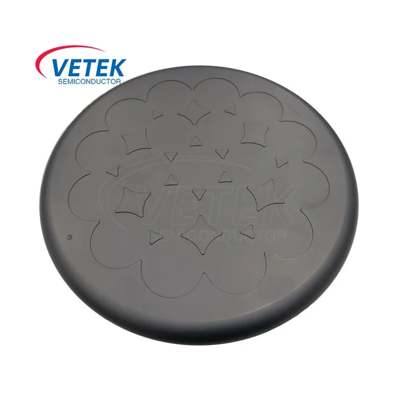
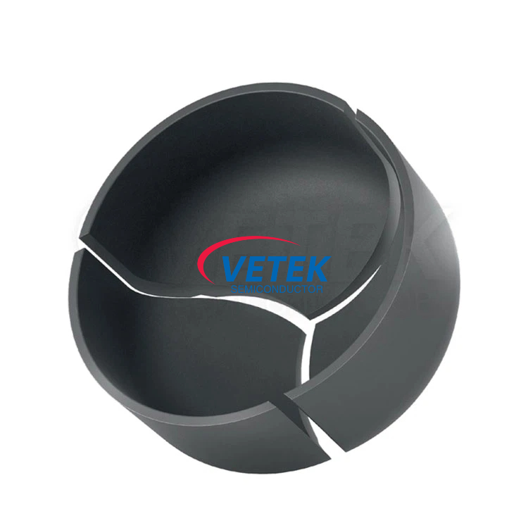
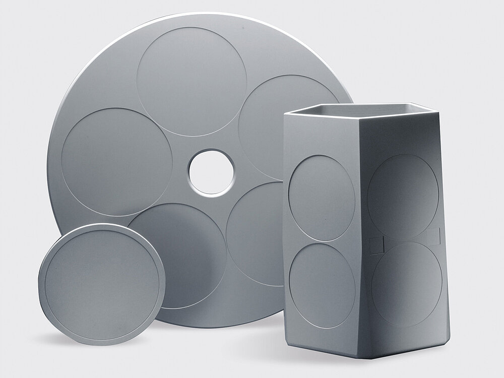
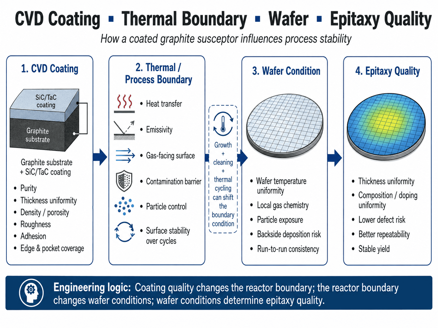
Introduction: In epitaxy, a coated graphite susceptor is part of the reactor’s thermal, chemical and contamination boundary. Its value lies not in coating thickness alone, but in how consistently the finished part preserves wafer temperature, surface stability and repeatability through growth and cleaning cycles.
Core conclusion: Even with unchanged temperature, pressure and gas flow, coating roughness, deposits, pocket geometry or interface degradation can alter heat transfer and surface chemistry. The coated susceptor should therefore be treated as a process-critical reactor component, not a passive wafer holder.
Typical growth temperatures illustrate the load: GaN MOCVD often runs near 1000–1100°C, Si epitaxy around 1050–1200°C, and SiC epitaxy roughly 1500–1700°C. Wafer temperature depends on heater power plus susceptor geometry, emissivity, pocket depth, rotation and gas flow.
Planetary MOCVD uses laminar flow and multiple carrier rotation to improve thickness, composition and doping uniformity.[1]
Core conclusion: “100 μm coating” is not a complete semiconductor specification. Density, purity, microstructure, roughness, CTE, thickness distribution, adhesion and defect control must be considered together, especially at pockets, edges, holes and shadowed features where local deposition may differ.
|
Parameter |
CVD SiC |
CVD TaC |
|
Density |
~3.2–3.21 g/cm³ |
~14.3 g/cm³ |
|
CTE |
~4.3–4.5×10⁻⁶/K |
~6.3×10⁻⁶/K |
|
Hardness |
~40–42 GPa |
~2000 HK |
|
Thickness |
~100 μm typical |
≥20 μm; ~35±10 μm |
|
Roughness |
~1–3 μm, process dependent |
Process dependent |
|
Purity |
>6N possible |
Grade dependent |
The engineering chain is:
CVD temperature / pressure / gas ratio → grain growth → density / roughness / stress → coating life.
Higher pressure increased roughness and porosity, while excessive temperature produced coarser structures.[3]
Core conclusion: A coating can become process-unacceptable before it visibly peels. Thickness drift, recession, deposits or roughness change can alter wafer-to-susceptor heat transfer and emissivity, creating temperature or run-to-run drift while the component still appears mechanically intact.
Wafer heat balance:
Qtotal = Qconduction + Qradiation + Qconvection
The coated susceptor influences these terms through material properties, surface condition and geometry. Pocket depth matters because coating buildup changes the final wafer seating geometry.
A nominal 100 μm coating that varies around a pocket can change both local thermal path and final dimensions. Small variation does not automatically cause non-uniformity, but post-coating pocket depth should be a CTQ.
During production:
growth deposits + cleaning + thermal cycling → roughness/emissivity drift → thermal-boundary drift → wafer-temperature drift → growth-rate/composition drift.
Component lifetime should therefore be defined by process limits—not simply by “no visible breakage.”
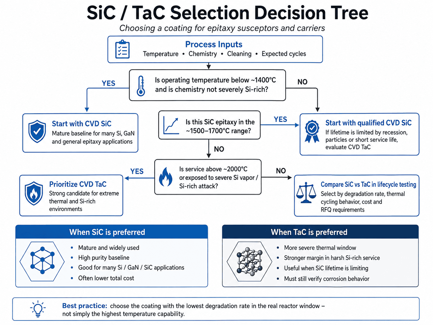
Core conclusion: CVD SiC is the practical baseline for many Si, GaN and SiC epitaxy parts because of its maturity, purity and compatibility with graphite. TaC becomes attractive when extreme temperature or Si-rich chemistry makes SiC recession the verified lifetime-limiting mechanism.
|
Process Window |
Starting Choice |
Engineering Logic |
|
Si epitaxy, ~1050–1200°C |
CVD SiC |
Mature, sufficient margin |
|
GaN MOCVD, ~1000–1100°C |
CVD SiC |
Established carrier surface |
|
SiC epitaxy, ~1500–1700°C |
SiC first; evaluate TaC if life-limited |
Higher severity |
|
Severe Si-rich attack |
Evaluate TaC |
Higher refractory margin |
|
>2000°C hot-zone service |
TaC strongly considered |
SiC stability may limit life |
→ Yes: qualify CVD SiC.
→ No: continue.
SiC epitaxy at ~1500–1700°C?
→ Start with proven SiC. If recession, particles or short life dominate, compare TaC.
>2000°C or severe Si-vapor exposure?
→ Prioritize TaC evaluation.
TaC is not chemically invulnerable. At 1973 K in silicon vapor, CVD TaC formed TaSi₂/SiC reaction products; increasing Si exposure increased corrosion depth and roughness.[4] Selection should therefore be based on degradation rate in the real reactor, not melting point alone.
Core conclusion: Most coated-susceptor failures arise from coupled thermal stress, deposition non-uniformity, chemical recession and cleaning or handling damage. Failure analysis should link the visible defect to its root mechanism and then to the wafer symptom instead of stopping at “coating peeling.”
|
Failure Mode |
Root Mechanism |
Main Process Risk |
|
Microcracking |
CTE mismatch + thermal cycling |
Gas ingress, particles |
|
Delamination |
Residual stress / weak interface |
Flaking |
|
Pinhole/porosity |
Incomplete densification |
Graphite exposure |
|
Edge chipping |
Stress/handling |
Local particles |
|
Chemical recession |
High-T reactive chemistry |
Roughness/emissivity drift |
|
Deposit buildup |
Parasitic deposition |
Thermal/flow drift |
A useful first-order thermal-stress relation is:
σ ≈ E × Δα × ΔT
where E is coating modulus, Δα the coating/substrate CTE difference and ΔT the thermal excursion. This is why graphite CTE matching matters almost as much as coating purity.
Deep pockets, holes and grooves can receive different precursor transport:
local thin/porous coating → thermal/chemical attack → graphite exposure → erosion → particles → wafer-defect risk.
A component may therefore reach process end-of-life before mechanical end-of-life.
Core conclusion: Qualification should convert reactor conditions into measurable CTQs and verify them on the finished geometry. Material certificates alone are insufficient; the target is repeatable coating integrity, dimensions and thermal/chemical behavior through representative growth and cleaning cycles.
A practical specification should include:
Recommended checkpoints:
Incoming → defined growth cycles → cleaning → end-of-life.
Correlating these checkpoints with particle and wafer data is more useful than visual inspection alone.
How thick should CVD SiC be?
Around 100 μm is a useful reference, not a universal optimum. Geometry, corrosion allowance, stress and dimensional tolerance determine the target.
Does thicker coating always last longer?
No. It adds corrosion reserve but may also increase residual stress and dimensional shift.
Why does SiC coating peel?
Typical contributors are CTE mismatch, residual stress, interface defects, edge geometry, thermal cycling, chemical attack and cleaning damage.
When should TaC replace SiC?
When high-temperature or Si-rich attack is proven to be the dominant SiC lifetime limit and TaC gives a better lifecycle result.
Core conclusion: CVD-coated graphite should be qualified as part of the epitaxy process. The target is stable thermal, chemical and dimensional behavior throughout production, with end-of-life defined by measurable process CTQs rather than visible damage alone.
The engineering chain is:
graphite substrate → CVD microstructure → finished geometry → thermal/chemical stability → wafer repeatability.
The better question is not simply “How thick is the coating?” but “How will this component behave after repeated growth, cleaning and thermal cycles, and what measurable limit defines its end of life?”
References
[1] AIXTRON SE, Planetary Principle (MOCVD).
[2] SGL Carbon, SIGRAFINE® SiC Coating – Material Data.
[3] Huo Y. et al., Scientific Reports 16, 4150 (2026), “Study of the Process-Structure-Property Correlation in CVD-SiC Coatings on Graphite Substrates.”
[4] Hao K. et al., Vacuum 241, 114677 (2025), “Silicon Vapor Induced Corrosion Mechanisms of CVD TaC Coatings on Graphite Substrates.”
Engineer Nickwu has 15 years of experience in the R&D of CVD coatings and carbon-based hot-zone materials. He led the project to introduce mass production for China's first TaC-coated graphite components used in 8-inch SiC epitaxy. He has participated in numerous hot-zone design and failure analysis projects for SiC crystal growth and holds seven invention patents related to hot-zone materials.
+86-579-87223657
Wangda Road, Ziyang Street, Wuyi County, Jinhua City, Zhejiang Province, China