
QR Code
Products
Contact Us


Fax
+86-579-87223657

E-mail

Address
Wangda Road, Ziyang Street, Wuyi County, Jinhua City, Zhejiang Province, China
Key Conclusions: In the 8-inch era, competitive advantage comes from yield per furnace, and yield is decided by what happens in the hot zone — long before any wafer processing begins.
Two years ago, 8-inch SiC was a roadmap slide. Today it is the market reality. More than 20 companies were building or planning 8-inch SiC lines in 2025, and at least eight more joined in the first half of 2026. Wolfspeed's 8-inch device revenue grew 103% in 2025. Semixlab Technology expects its 8-inch shipments to grow 500–800% this year. By 2028, industry analysts expect 8-inch wafers to outsell 6-inch, with the SiC market approaching US$10 billion.
TrendForce describes an industry entering a 2–3 year digestion phase — 6-inch capacity may be in surplus, but high-yield 8-inch capacity remains scarce. Yield, not capacity, is now the moat. And yield has an address: the hot zone of the furnace.
Key Conclusions: Most unexplained 8-inch yield loss is a thermal-field problem in disguise — and the thermal field is only as stable as the coating protecting the graphite.
The economics of the 8-inch move are simple: about 78% more usable wafer area per crystal. The physics are less forgiving. Scaling the graphite hardware to 200 mm amplifies three failure modes that barely registered at 6 inches:
· Susceptor warpage. Rapid thermal cycling across a 200 mm graphite part produces microscopic deformation. Edge defects — the dominant yield killer in current 8-inch lines — trace back to this warpage more often than to source-powder quality.
· Thermal uniformity drift. A degrading fixture cannot hold a stable temperature profile across a larger crucible. The crystal sees a moving thermal field, and the growth front responds with stress and defects.
· Slow contamination. 8-inch campaigns run hotter and longer. Every microgram of impurity an under-protected graphite part releases becomes micropipes, etch pits, and dislocations — the difference between a sellable boule and scrap.
None of these show up in a wafer inspection report as "fixture failure." They show up as yield loss with no obvious cause, which is what makes them expensive.
Key Conclusions: Above 1,600°C, TaC is not a premium upgrade over SiC coating — it is the only coating chemistry that holds the line on purity and dimensional stability for a full 8-inch campaign.
SiC coatings on graphite have earned their place in silicon epitaxy and moderate-temperature processes. But PVT growth at 2,200–2,400°C and high-temperature MOCVD push fixtures into a regime where SiC coating chemistry works against you:
· Above roughly 1,600°C, SiC coatings react with hydrogen, driving graphite outgassing and downstream defects
· TaC corrosion rates run about 6× lower than SiC coating in high-temperature ammonia, and more than 10× lower in high-temperature hydrogen — the two atmospheres that dominate modern growth chambers
· Parts that SiC coating survives for dozens of thermal cycles, TaC coating survives for hundreds
|
Property |
TaC Coating |
Why it matters at 8 inches |
|
Melting point |
~3,880°C — highest of all binary carbides |
Stable service at 2,300–2,600°C |
|
Chemical inertness |
Resists H₂, NH₃, SiH₄, Si vapor |
Purity holds through full campaigns |
|
Hardness |
15–20 GPa |
Withstands gas erosion, protects against particles |
|
Thermal conductivity |
~22 W/(m·K), matched to graphite |
Thermal field stays uniform as the part ages |
|
Purity ceiling |
<5 ppm achievable |
Transition metals stay out of the epi layer |
Key Conclusions: A longer-lasting hot zone is not a maintenance saving — it is recovered furnace uptime, recovered crystals, and yield your competitors lose while their furnaces are open.
The money argument is blunt. Opening a furnace early for maintenance costs you the fixture, the ramp-up time, the re-stabilized thermal field, and whatever crystal was mid-growth. Industry analyses put fixture replacement at every 50–200 growth cycles, and note that fewer than 10 qualified TaC coating suppliers exist worldwide — one reason wafer producers are actively qualifying second sources.
Field data shows what a robust TaC system delivers:
· In PVT service at SiCrystal (Rohm Group), CVD TaC-coated graphite components and pyrolytic carbon coatings extended crucible reuse to 200 hours with zero high-temperature weight loss, and measurably reduced micropipe and etch-pit densities
· In GaN/SiC epitaxy, TaC-coated fixtures have delivered 2–3× the lifespan of SiC-coated equivalents
· Chinese programs have now demonstrated TaC-coated parts exceeding 600 hours of service life — the supply base has moved well past lab curiosity
The pattern is consistent: when the hot zone stays stable, yield follows. When it doesn't, no amount of downstream tuning recovers the loss.
Key Conclusions: Qualify on auditable evidence — lot-level purity reports, bonding data, and named equipment platforms — never on a datasheet alone.
An 8-inch susceptor is not a scaled-up 6-inch part. The larger coating area magnifies every challenge in thickness uniformity, adhesion, thermal stress, warpage, and particle release. Before you commit a production line to a supplier, press on five points:
1. Large-format capability, proven not projected. Ask what diameter they coat in production, not in principle. Facilities coating up to Ø750 mm keep 8-inch hardware well inside the process window; Ø200 mm parts at the edge of a supplier's capability are a risk you will pay for later.
2. Purity data you can audit. Request GDMS and D-SIMS reports on actual lots. Best-in-class CVD TaC runs at 99.99953% purity, with transition elements (Fe, Ni, Cu) below 1 ppm.
3. Adhesion engineering. Buffer-layer technology with bonding strength above 3 MPa and a CTE matched to graphite is what stops delamination across hundreds of ambient-to-2,300°C cycles. A coating that peels at run 40 is worse than no coating.
4. Conformal coverage on real geometries. A uniform 30–40 μm layer must hold across planetary susceptors, covers, diversion rings, and halfmoon parts — not just flat test coupons.
5. Production history on your tools. Field experience on AIXTRON G5/G10, LPE, ASM, and leading PVT platforms, backed by 3 μm-class machining and in-house GDMS, SEM, XRD, and scratch testing, tells you the supplier has already solved the problems you are about to meet.
The 8-inch transition rewards companies that treat thermal-field materials as strategic. The substrate makers reporting yields that justify their capex are the ones whose hot zones stay stable for hundreds of hours; the ones treating coated hardware as a purchasing line item are the ones staring at edge-defect maps.
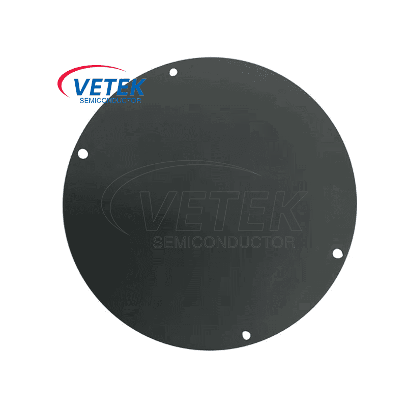
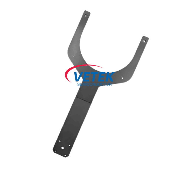
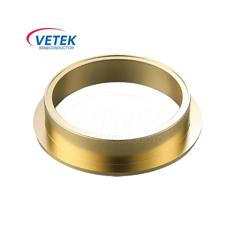
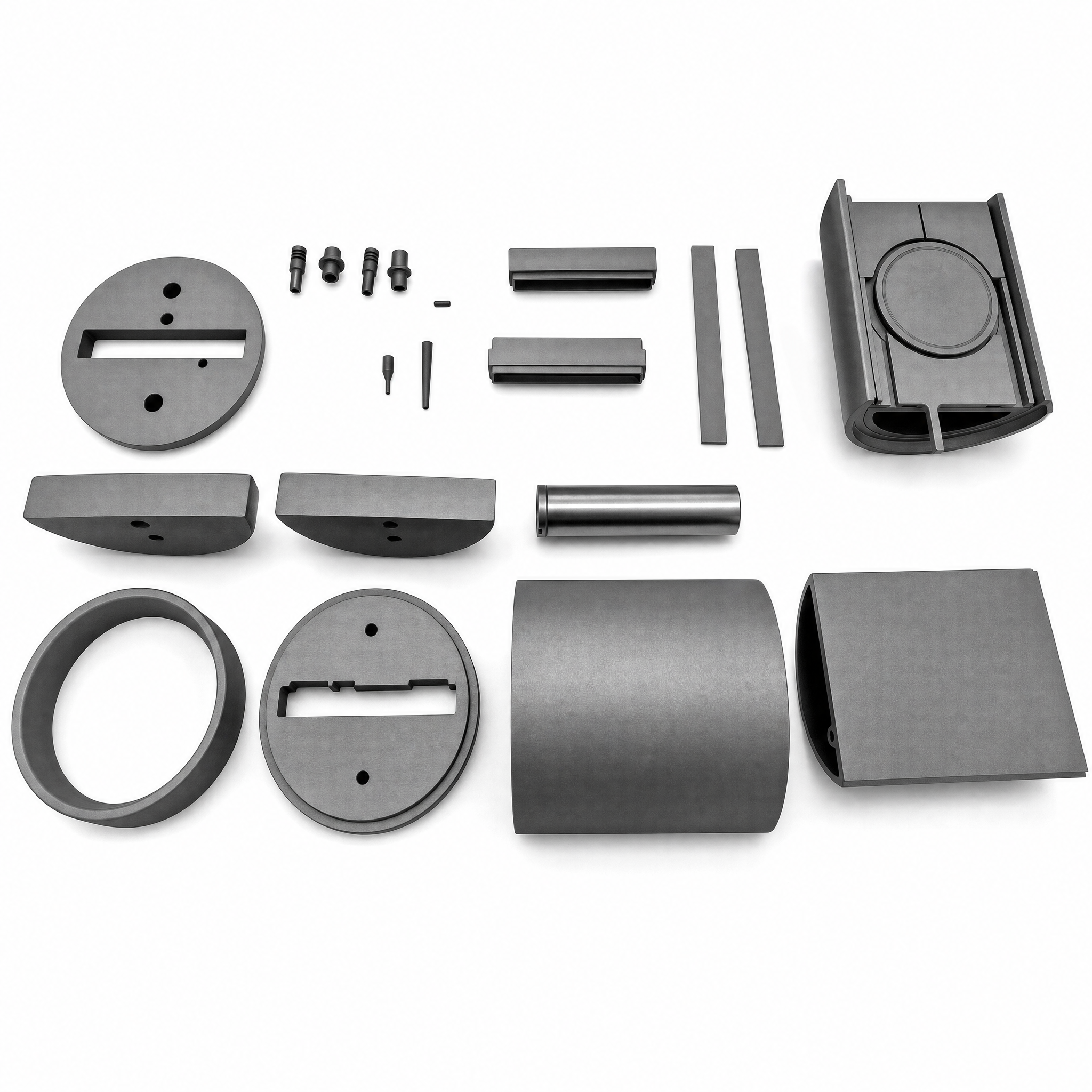
At VeTek Semiconductor, we manufacture CVD TaC-coated graphite components — planetary and wafer susceptors, susceptor covers, crucibles, and porous TaC for sublimation control — at 99.99953% coating purity, >3 MPa bonding strength, 30–40 μm conformal coverage, and coating capability up to Ø750 mm. Our parts run in production on AIXTRON, LPE, and ASM platforms, and delivered 200-hour crucible reuse in high-corrosion PVT service at a Rohm Group substrate company. Every part ships with GDMS/D-SIMS traceability from dual R&D centers where R&D investment exceeds 30% of annual revenue.
Qualifying components for an 8-inch ramp, or looking for a second source to de-risk your hot-zone supply chain? Contact our engineering team for a sample evaluation on your furnace and process parameters. Standard parts ship from stock; custom parts typically deliver in 3–6 weeks.
Q1: What temperature can a TaC coating withstand?
Tantalum carbide melts at roughly 3,880°C — the highest of all binary carbides. In production, TaC-coated graphite components serve continuously at 2,300–2,600°C in corrosive H₂ and NH₃ atmospheres.
Q2: How long does a TaC-coated graphite crucible last in PVT growth?
Documented field results reach 200 hours of crucible reuse with zero high-temperature weight loss, and leading programs have exceeded 600 hours of coating service life. Typical replacement intervals run 50–200 growth cycles depending on the process.
Q3: When should I choose TaC over SiC coating?
Below ~1,600°C, SiC coating remains a sound, economical choice. For SiC PVT crystal growth and high-temperature MOCVD epitaxy — where hydrogen and ammonia attack the fixture — TaC's 6–10× lower corrosion rate and longer thermal-cycling life make it the safer engineering decision.
References:
1. Wolfspeed. "2025 Fiscal Year Report - China Market 8-Inch Device Revenue Growth." 2025.
2. TrendForce. "Global SiC Power Device Market Analysis Report 2026." Report No. RP260401AC, 2026.
3. Momentive Technologies. "TaC Coatings for High-Temperature Semiconductor Applications." Technical Data Sheet, 2025.
Engineer Nickwu has 15 years of experience in the R&D of CVD coatings and carbon-based hot-zone materials. He led the project to introduce mass production for China's first TaC-coated graphite components used in 8-inch SiC epitaxy. He has participated in numerous hot-zone design and failure analysis projects for SiC crystal growth and holds seven invention patents related to hot-zone materials.


+86-579-87223657


Wangda Road, Ziyang Street, Wuyi County, Jinhua City, Zhejiang Province, China
Copyright © 2024 WuYi TianYao New Material Tech.Co.,Ltd. All Rights Reserved.
Links | Sitemap | RSS | XML | Privacy Policy |