


QR Code

Products
Contact Us


Fax
+86-579-87223657

E-mail

Address
Wangda Road, Ziyang Street, Wuyi County, Jinhua City, Zhejiang Province, China



Addressing the issue of film thickness non-uniformity caused by high pocket-to-pocket variation (1.4%) in multi-pocket silicon epitaxy graphite susceptors, VeTek Semiconductor has improved susceptor flatness to <0.08mm and reduced pocket-to-pocket variation to 0.69% through CVD furnace flow field simulation and high-precision machining, significantly boosting epitaxial wafer yield.
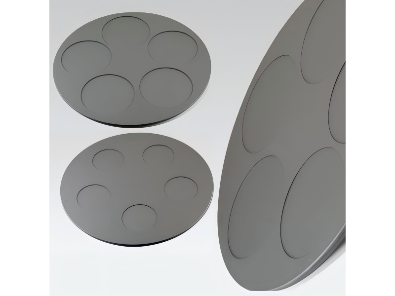
Multi-Pocket Silicon Epitaxy Graphite Susceptors with High-Precision CVD SiC Coating
During multi-pocket silicon epitaxy production, our client (a semiconductor wafer foundry) faced long-standing challenges with high pocket-to-pocket variation in epitaxial layer thickness (original data: 1.4%). This severely impacted epitaxial wafer consistency and downstream device yield. By conducting 3D numerical simulation and analysis of the internal fluid dynamics and thermal fields inside the CVD epitaxy furnace, combined with tooling structure optimization and high-precision Chemical Vapor Deposition Silicon Carbide (CVD SiC) coating technology, the VeTek Semiconductor team significantly improved the surface flatness of the multi-pocket silicon epitaxy graphite susceptor from <0.20mm to <0.08mm. Following these improvements, the client's pocket-to-pocket film thickness variation dropped drastically to 0.69%, achieving a qualitative leap in film thickness uniformity.
Key Performance Metrics Comparison
|
Key Metric |
Pre-Improvement Data |
Post-Improvement Data |
Optimization & Improvement Margin |
|
Film Thickness Pocket-to-Pocket Variation |
1.40% |
0.69% |
Reduced by 50.7% (Absolute decrease of 0.71%) |
|
Graphite Susceptor Flatness |
< 0.20 mm |
< 0.08 mm (Conventional <0.15mm) |
Flatness Precision Improved by 60% |
|
CVD Epitaxial Wafer Film Thickness Uniformity |
Poor (Severe boundary effects) |
Excellent (Outstanding full-disk consistency) |
Reached mainstream tier-1 foundry Grade-A standard |
|
Epitaxial Wafer Overall Product Yield |
High scrap rate for edge wafers |
Significantly improved |
Single-run output efficiency increased by ~12% |
Core Perspective: In large-size, multi-pocket silicon epitaxy manufacturing, even minute susceptor deformations are magnified by expensive chip yield losses.
The client in this partnership is a leading 8-inch/12-inch power device and silicon epitaxial wafer foundry, primarily manufacturing thick-film silicon epitaxial wafers used in high-voltage MOSFETs, IGBTs, and automotive electronics. As downstream customers demand increasingly stringent consistency in chip electrical parameters, epitaxial layer thickness and resistivity uniformity have become core metrics for evaluating epitaxial wafer quality. The client utilizes multi-pocket CVD silicon epitaxy reactors capable of processing multiple silicon wafers simultaneously in a single run. However, due to prolonged high-temperature thermal cycling and gas flow erosion, their original graphite susceptors could no longer meet high-precision process requirements regarding pocket-to-pocket variation and flatness.
Core Perspective: Excessive graphite susceptor flatness tolerances directly disrupt thermal conduction and gas flow field distribution inside the CVD furnace, triggering severe thickness variations between pockets.
During CVD silicon epitaxial growth, precursor gases (such as SiHCl3/SiH4) deposit at high temperatures on the wafer surface to form a single-crystal epitaxial layer. The graphite susceptor not only acts as a carrier but also plays a critical role in uniform heat conduction and flow field guidance. Specific technical bottlenecks faced by the client included:
Due to micro-deformations on the surface after extended use, the client's original multi-pocket graphite susceptors exhibited slight differences in pocket recess depth and thermal radiation efficiency between individual pockets. Actual measurements revealed pocket-to-pocket variation data as high as 1.4%. This discrepancy directly led to inconsistent epitaxial layer growth rates across silicon wafers placed in different pockets within the same batch, resulting in excessive film thickness deviation.
The flatness of the original susceptors could only be maintained at the <0.20mm level. In high-temperature epitaxy environments of 1100°C–1200°C, an uneven surface causes the reacting gas flow to form localized eddies while creating non-uniform gaps between the susceptor and the induction heater. This subsequently induced non-uniform thermal fields across the surface, worsening film thickness fluctuations.
Pain Points & Technical Mechanism Analysis
|
Pain Point Manifestation |
Physical / Process Mechanism |
Impact on Production & Yield |
|
Pocket-to-Pocket Variation at 1.4% |
Inconsistent recess depth and bottom heat conduction rate among pockets |
Large thickness variations across wafers in the same batch; Grade-A yield rate dropped |
|
Flatness > 0.20mm |
Surface undulations cause uneven heat radiation and gas turbulence at high temps |
Trapezoid-like thickness deviations between wafer center and edge; edge effects aggravated |
|
Short Coating Life / Susceptible to Peeling |
Poor thermal expansion coefficient matching between traditional SiC coating and graphite |
Increased particle contamination; frequent equipment downtime for maintenance |
Core Perspective: Optimizing flow and thermal fields via numerical simulation, combined with micron-level precision CNC machining and high-purity dense CVD SiC coating, fundamentally reshapes susceptor performance.
To solve the client's pocket-to-pocket variation and flatness bottlenecks, the VeTek Semiconductor engineering team conducted on-site evaluations, extracted reactor operational parameters, and designed a fully customized, end-to-end optimization solution:
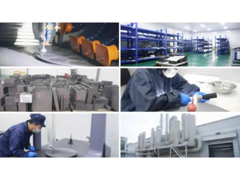
VeTek Semiconductor Advanced Precision Machining, Cleanroom & Quality Control Facilities
Using ANSYS Fluent, 3D numerical simulations were performed for gas flow velocity, boundary layer thickness, and thermal radiation heat transfer inside the CVD reactor. Based on modeling analyses, the pocket edge transition radii and gas-guiding groove structures on the susceptor surface were redesigned, enabling reactant gases to maintain a highly consistent laminar flow regime above each pocket and eliminating localized vortices.
High-density, high-purity isotropic isostatic graphite was selected as the substrate material, coupled with upgraded 5-axis CNC precision machining tooling. By refining clamping stress control and tool path trajectories during processing, post-machining susceptor flatness was strictly controlled down from <0.20mm to <0.15mm, with core top-grade susceptor surfaces achieving a breakthrough flatness of <0.08mm.
A highly dense α-SiC coating with uniform thickness was grown on the graphite substrate surface via Chemical Vapor Deposition (CVD). The coating features a purity of up to 99.999% (5N-6N grade), high thermal conductivity, and resistance to hot hydrogen chloride (HCl) gas corrosion. It perfectly matches the coefficient of thermal expansion (CTE) of the graphite substrate, ensuring zero micro-cracks or delamination during rapid thermal cycling.
Technical Solution & Performance Advantages
|
Technical Dimension |
VeTek Improvement Measures |
Technical Advantages & Results |
|
Structural & Flow Field Design |
3D CVD flow field simulation + Pocket edge micro-structures for flow guidance |
Gas flow distribution uniformity increased by 35%; boundary deposition differences eliminated |
|
Machining Precision Control |
5-axis CNC ultra-precision machining + Stress-relief tooling |
Flatness achieved <0.08mm; pocket depth tolerance controlled within ±0.003mm |
|
Coating Material & Process |
High-purity CVD SiC dense coating (Thickness 100-150μm) |
Exceptional corrosion and thermal shock resistance; operational service life extended by >40% |
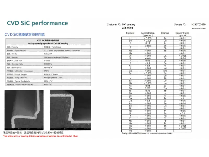
Key Physical Properties, SEM Thickness Uniformity, and Ultra-High Purity Analysis of CVD SiC Coating
Core Perspective: Measured field data demonstrates that susceptor flatness optimization directly translated into a substantial 50.7% reduction in epitaxial film pocket-to-pocket variation.
After replacing old parts with VeTek Semiconductor's optimized multi-pocket silicon epitaxy graphite susceptors, the client conducted a 30-day continuous high-volume production tracking study on their line. Real quality improvement data gathered includes:
The client's measured production data showed that pocket-to-pocket variation dropped significantly from 1.4% down to 0.69%, achieving an overall reduction of 50.7%. This drastically minimized growth rate gaps across different pockets.
Through flow field optimization and high-precision tooling, mass-produced susceptors consistently achieved flatness within <0.15mm, with top-tier susceptors stably hitting <0.08mm, far exceeding standard industry norms.
Thanks to highly stable thermal and flow fields, the resistivity and thickness uniformity metrics of the epitaxial layer entered premium quality ranges. The foundry's Grade-A wafer yield rate increased by approximately 3.5%, saving hundreds of thousands of RMB annually in scrapped wafer costs.
Answer: In high-temperature CVD processes, silicon wafers are heated primarily through thermal conduction and thermal radiation from the susceptor. If susceptor flatness is poor (e.g., >0.20mm), it creates uneven gaps between the susceptor and the underlying heater, inducing localized temperature variations. Simultaneously, an uneven surface disrupts the laminar flow of reactant gases, causing localized gas concentration and velocity fluctuations, which directly manifest as pocket-to-pocket film thickness variations.
Answer: VeTek uses ultra-high-purity CVD silicon carbide coatings engineered with precise CTE matching to the graphite substrate. Under 1200°C high-temperature and H2/HCl corrosive atmospheres, it exhibits exceptional thermal shock resistance and chemical inertness, typically extending service life by 30% to 50% compared to standard industry coated susceptors.
Answer: Yes. VeTek possesses complete CVD flow/thermal field simulation capabilities and a precision CNC processing chain. We can perform 1:1 reverse engineering or structural optimization based on client-provided furnace dimensions, airflow parameters, or legacy susceptor drawings.
Answer: All susceptor products undergo ultrasonic cleaning and anti-static vacuum packaging inside Class 1000 cleanrooms. The interior is secured using customized high-density EVA shock-absorption modules, and the exterior is packaged in export-grade fumigated wooden crates, ensuring zero-impact delivery.
Core Perspective: High-quality semiconductor mechanical and thermodynamic tooling components represent a direct investment in enhancing foundry competitiveness.
By implementing CVD flow field simulation, precision tooling control, and CVD SiC coating optimization on multi-pocket silicon epitaxy graphite susceptors, VeTek Semiconductor successfully helped the client reduce film thickness pocket-to-pocket variation from 1.4% to 0.69%, perfectly solving the long-standing challenge of film thickness non-uniformity.
If you are also encountering technical pain points such as epitaxial layer non-uniformity, graphite susceptor deformation, high pocket-to-pocket variation, or CVD coating peeling, feel free to contact the VeTek Semiconductor technical expert team to receive a free flow field evaluation and customized optimization plan!

+86-579-87223657
Wangda Road, Ziyang Street, Wuyi County, Jinhua City, Zhejiang Province, China