




QR Code

Products
Contact Us


Fax
+86-579-87223657

Email

Address
Wangda Road, Ziyang Street, Wuyi County, Jinhua City, Zhejiang Province, China



|
Evaluation Dimension / Item |
Detailed Engineering Parameters & Value Delivered |
|
Industry |
Semiconductor Manufacturing, Microelectronics Packaging, Optical Communications, Technical Ceramics (GTMS/CTMS Hermetic Sealing Field) |
|
Process |
GTMS/CTMS Glass/Ceramic-to-Metal Hermetic Sealing High-Temperature Sintering, CTE Precise Thermal Matching Clamping |
|
Solution |
Ultra-High-Density Micro-Hole Special Graphite Fixture Plate (Single plate area < 0.01 ㎡, arrayed with nearly 1,500 micro-holes; total set contains nearly 10,000 micro-holes) |
|
Services |
Material Selection & CTE Thermal Matching Analysis, Micro-Hole Deep Machining Tool Path Design, Engineering Technical Documentation, Batch Manufacturing & Full Inspection |
|
Results |
• Overcame the continuous deep-hole machining bottleneck for 10,000 holes over 10 months, achieving micron-level zero-defect control |
During the GTMS/CTMS high-temperature sintering process in microelectronics packaging, special graphite fixtures must combine micron-level fit with high thermal resistance and stability. To address the challenges of edge chipping, ultra-fast tool wear, and cumulative tolerance in small-area ultra-high-density micro-holes, VeTek spent 10 months breaking through the bottleneck of continuous deep machining for nearly 10,000 micro-holes through material adaptation, cutting kinematics reconstruction, and closed-loop multi-dimensional inspection, realizing highly reliable one-stop delivery.
|
Core Conclusion: Through orthogonal optimization of process parameters for micro-hole deep machining and graphite selection based on CTE thermal matching, the micro-hole machining yield leaped from batch scrap risk to a stable delivery rate of over 98.5%. |
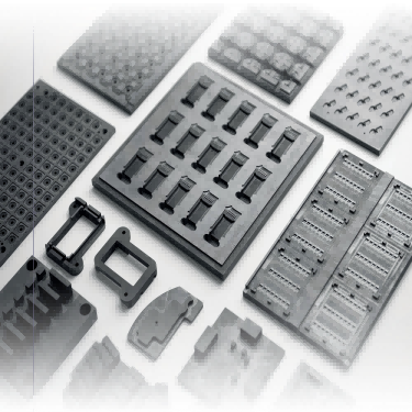
Figure 1 - GTMS/CTMS special graphite fixture plate and micro-hole machining structural components
In the GTMS hermetic packaging process, hole consistency and thermal deformation resistance of graphite fixture plates directly determine packaging hermeticity and finished product yield. Key process and performance indicators before and after the VeTek team's technical breakthrough are compared as follows:
|
Evaluation Dimension |
Before Improvement (Original Process Status) |
After Improvement (VeTek Optimized Solution) |
|
Single-Plate Micro-Hole Density |
Nearly 1,500 holes / 0.01 ㎡ (Machining highly prone to chipping) |
Nearly 1,500 holes / 0.01 ㎡ (Micron-level zero-defect forming) |
|
Continuous Machining Tool Wear Rate |
Wear exceeded standard every 200 holes, causing hole diameter drift |
Dedicated coating & path optimization, tool wear rate reduced by 65% |
|
Coefficient of Thermal Expansion (CTE) Matching |
Conventional graphite thermal expansion was relatively high, leading to pin deviation |
Precisely matched Kovar alloy expansion curve |
|
Overall Acceptance Pass Rate |
Frequent scrap due to micron-level tolerance exceeding limits (<60%) |
Stable batch delivery standard (≥98.5%) |
|
Core Conclusion: High-density pin glass-to-metal sealing imposes near-limit demands on the microscopic geometric precision and high-temperature cleanliness of special graphite fixtures. |
The customer in this cooperation is an R&D and manufacturing enterprise specializing in high-reliability sensors and microelectronics packaging components. Its core production lines widely apply GTMS/CTMS (Glass/Ceramic-To-Metal Seal) sintering processes. In high-temperature sealing furnaces, special graphite fixtures serve as high-precision carrier molds, responsible for precisely positioning and holding hundreds to thousands of fine metal pins (such as Kovar alloy) and glass preforms. Since a single graphite fixture plate in this project measures less than 0.01 square meters yet must precisely accommodate nearly 1,500 micro-holes, the complete fixture set integrates nearly 10,000 micro-holes with extremely thin walls between holes. During high-temperature sintering at 800°C–1000°C, any slight out-of-tolerance hole diameter, positional deviation, or graphite dust detachment will directly lead to metal pin tilt, glass insulation cracking, or even complete loss of hermeticity.
|
Core Conclusion: High brittleness of graphite material, rapid wear of micro-holes, and micron-level cumulative tolerances are the core triggers leading to batch scrap of 10,000-hole level graphite fixtures. |
Prior to bringing in the VeTek technical taskforce, the customer encountered severe technical bottlenecks during trial production and small-batch processing: First, micro-hole edge chipping and tearing: Graphite is a porous brittle material; during continuous drilling of high-density micro-holes, shear stress at the moment the micro-drill enters and exits easily induces brittle edge chipping at the hole mouth. Second, tolerance drift caused by tool micro-wear: When processing thousands of micro-holes continuously, wear on fine drill bits intensifies, causing hole diameters in deep holes to exhibit a tapered gradient, where a deviation of just a few microns leads to the failure and scrapping of the entire fixture set containing nearly 10,000 holes. Third, thermal expansion mismatch and dust contamination: The high-temperature CTE of ordinary graphite materials does not match that of metal pins, and fine dust easily sloughs off, contaminating the glass sintering interface.
|
Core Conclusion: Through tool path algorithm optimization, dynamic cutting speed compensation, and dedicated anti-chipping coated micro-drills, the challenges of micro-hole edge chipping and deep-hole tolerance accumulation are completely overcome. |
To address the difficulties of deep machining 10,000 micro-holes, the VeTek R&D team reconstructed the cutting kinematics model and implemented systematic process engineering:
· Tool Path Algorithm & Plunge Feed Reconstruction: Optimized feed speed and segmented rotational speed through orthogonal experiments, adopting a micro-feed pulsed plunge strategy to effectively reduce machining impact shear force by over 45%, completely eliminating hole mouth chipping defects.
· Anti-Chipping Micro-Drills & Chip Removal Flow Field Optimization: Customized ultra-fine grain diamond-coated micro-drills combined with a pulsed negative-pressure micro-cooling chip removal system increased tool wear resistance lifetime by more than 3 times, ensuring hole diameter drift across 1,500 micro-holes per single plate remains under ±0.002 mm.
|
Process Parameter / Dimension |
Original Process |
VeTek Optimized Process |
|
Micro-Hole Machining Feed Strategy |
Constant high-speed continuous plunge (High impact force) |
Segmented phased speed + Micro-feed pulse strategy |
|
Micro-Drill Tool Selection |
Conventional uncoated micro tungsten carbide drill |
Proprietary ultra-fine grain anti-chipping diamond-coated micro-drill |
|
Deep-Hole Chip Removal & Cooling |
Conventional air-blowing chip removal (Dust residual accumulation) |
High negative-pressure pulse dynamic suction + Airflow micro-adjustment |
|
Hole Mouth Chipping Control |
Hole edge chipping rate > 8% |
Hole mouth complete and smooth, chipping rate < 0.05% |
|
Core Conclusion: Selected high-thermal-conductivity special graphite precisely matching Kovar alloy CTE establishes a closed loop of 'Optical + CMM' full inspection and ultrasonic cleaning, achieving zero-defect delivery of 10,000 holes. |
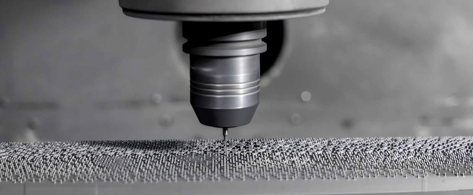
Figure 2 - Real details of special graphite fixture plate with zero surface chipping and high-precision micro-hole array
· Material Adaptation Solution: Strictly selected high-purity isostatic special graphite featuring a dense microstructure and excellent high-temperature thermal stability. Its Coefficient of Thermal Expansion (CTE) highly matches that of Kovar alloy, significantly suppressing high-temperature sintering thermal stress and micro-dust detachment.
· Collaborative Inspection & Deep Cleaning: The quality control line introduced a complementary system of 'Optical Image Measuring Instrument + Fully Automated Coordinate Measuring Machine (CMM)'. Optical imaging rapidly scans the spacing of the 10,000-hole array, while CMM verifies deep-hole perpendicularity and spatial groove locations; finally supplemented by multi-stage gradient ultrasonic cleaning to completely strip residual graphite impurities deep within micro-blind holes, reaching semiconductor-grade cleanliness.
|
Core Conclusion: Providing professional engineering answers regarding GTMS/CTMS fixture material selection, micro-hole tolerance limits, and high-temperature service life. |
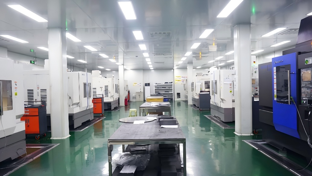
Figure 3 - VeTek High-Precision CNC Machining Center
Q: What are the minimum hole diameter and ultimate tolerances for micro-hole machining of high-density special graphite fixtures?
A: VeTek possesses micro-machining capabilities for hole diameters below 0.2 mm. Hole diameter tolerances can be stably controlled within ±0.003 mm, and true roundness as well as positional tolerances for 1,500 holes on a single plate reach ±0.005 mm, fully satisfying high-density pin GTMS packaging requirements.
Q: Why must GTMS hermetic sintering fixtures precisely match the CTE of Kovar alloy?
A: During the 800°C–1000°C sintering cycle, if the CTE of the fixture and metal pins are inconsistent, shear stress generated by cooling contraction will cause pin displacement, glass body cracking, or seal failure. Precise CTE matching ensures synchronized expansion and contraction, improving hermetic yield.
Q: How does the ultrasonic cleaning process ensure no residual graphite dust remains inside deep micro-holes?
A: We employ a multi-frequency gradient ultrasonic generation system combined with deionized water and specialized cleaning media. Utilizing high-frequency cavitation effects, fine graphite particles deep inside micro-holes and blind holes are completely stripped, followed by high-purity nitrogen blowing and vacuum drying to achieve semiconductor-level clean shipment.
In the field of semiconductor and microelectronics hermetic packaging, the micron-level machining precision and thermodynamic stability of carriers directly determine packaging yield and equipment utilization. Relying on continuous accumulation in high-purity materials, precision machining, and critical semiconductor component manufacturing, VeTek successfully overcame the industry-level manufacturing barrier of 1,500 micro-holes densely arrayed on a 0.01 ㎡ plate, realizing highly reliable mass-production delivery of 10,000-hole level special graphite fixtures.
As a manufacturing enterprise focused on the development of CVD SiC, TaC coatings, Solid SiC, and critical semiconductor materials and components, VeTek continuously provides high-performance material solutions for semiconductor manufacturing, crystal growth, and high-temperature process fields. At the same time, addressing application requirements in hermetic packaging, high-temperature sintering, and precision positioning, VeTek provides engineering services including high-purity graphite material selection, precision machining, and customized manufacturing support.
If you are seeking high-precision graphite components suitable for GTMS/CTMS hermetic sealing processes, or require material matching, structural optimization, and sample validation, please feel free to contact the VeTek engineering team. We will provide you with one-stop technical support from material selection to precision manufacturing.

Figure 4 - Panoramic View of VeTek Special Materials R&D and Precision Manufacturing Base
+86-579-87223657
Wangda Road, Ziyang Street, Wuyi County, Jinhua City, Zhejiang Province, China