





QR Code

Products
Contact Us


Fax
+86-579-87223657

E-mail

Address
Wangda Road, Ziyang Street, Wuyi County, Jinhua City, Zhejiang Province, China



VETEK Semiconductor is a high-tech enterprise specializing in high-temperature thermal field solutions for the photovoltaic and semiconductor industries. Founded in 2016, the company focuses on the research, development, and industrialization of high-temperature thermal field materials. We have independently mastered the core coating technologies of CVD Silicon Carbide (CVD SiC) and CVD Tantalum Carbide (CVD TaC), and have established a fully integrated manufacturing system covering graphite purification → precision machining → coating deposition.
The company has been recognized as a National Specialized and Sophisticated "Little Giant" Enterprise, ranking among the leading suppliers of semiconductor epitaxy thermal field solutions in China. Our products have successfully enabled the domestic substitution of key thermal field components for LED epitaxy, third-generation semiconductors, and silicon epitaxy, and have entered the core supply chains of multiple leading semiconductor manufacturers.
Key Message: Founded in 2016, VETEK Semiconductor is a National Specialized and Sophisticated "Little Giant" Enterprise. The company operates six dedicated business divisions, providing comprehensive solutions for the entire semiconductor high-temperature thermal field industry.
The company has more than 20 R&D professionals. Our core technical team comes from prestigious universities including Zhejiang University, Wuhan University, Central South University, and China University of Geosciences. The team possesses extensive expertise in:
· CVD equipment development
· Semiconductor material research
· Precision machining
· High-purity material preparation
· Quality management
The company consists of six major business divisions:
· Quartz & Ceramic Components Division
· Semiconductor Wafer Division
Key Message: Centered around critical semiconductor manufacturing processes, VETEK Semiconductor has established six mature product categories, including CVD SiC coatings, CVD TaC coatings, Solid Silicon Carbide (Solid SiC), high-purity graphite and carbon-based materials, quartz and advanced ceramics, and semiconductor wafers, covering major applications such as epitaxy, etching, and crystal growth.
Leveraging a stable Chemical Vapor Deposition (CVD) process, the company achieves high coating purity and excellent batch-to-batch consistency. These products are designed for long-term operation under high-temperature conditions.
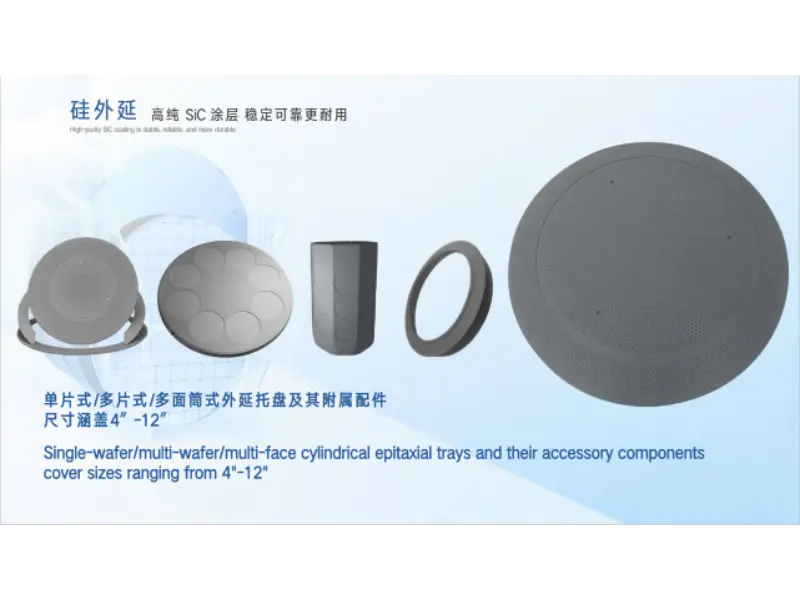
· SiC Coated Susceptor
· Wafer Carrier
· Planetary Disc
· Halfmoon
· Shower Head
· Barrel
· RTP Susceptor
· Wafer Lift Pin
· Various Process Components
· LPE
· Aixtron
· Veeco
· ASM
· Other mainstream epitaxy equipment platforms
To meet the increasingly demanding high-temperature and high-corrosion requirements brought by the rapid development of third-generation semiconductors, our TaC coatings are capable of operating continuously in environments exceeding 2300°C.
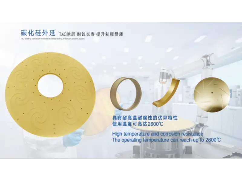
· TaC Coated Susceptor
· TaC Coated Heater
· TaC Crucible
· TaC Coated Graphite Parts
· SiC PVT Thermal Field Components
· SiC Single Crystal Growth
· Ultra-High-Temperature Thermal Field Systems
Solid Silicon Carbide combines high purity, excellent corrosion resistance, superior plasma resistance, and outstanding thermal stability, making it ideal for advanced etching systems and high-temperature furnace equipment.
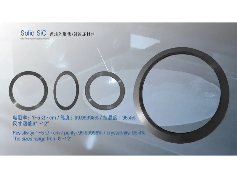
Main Products
· Focus Ring
· Edge Ring
· Shower Head
· Wafer Boat
· Furnace Tube
· Guide Cylinder
· Etching Components
We provide complete thermal field system solutions with products including:
· Graphite Susceptor
· Heater
· Crucible
· Heat Shield
· Graphite Ring
· Graphite Electrode
· Carbon Fiber Soft Felt
· Carbon Fiber Hard Felt
· Carbon Composite
All products can be custom-manufactured according to different equipment platforms.
Building upon our expertise in CVD material technologies, we have expanded our product portfolio to include:
High-Purity Quartz Products
· Quartz Boats
· Quartz Carriers
· Process Tubes
· Furnace Tubes
· Bell Jars
· Quartz Rings
· Quartz Flanges
· Gas Injection Tubes
· Quartz Crucibles
· Other customized quartz components
· High-Purity Alumina (Al₂O₃)
· Silicon Carbide (SiC)
· Silicon Nitride (Si₃N₄)
· Boron Nitride (BN)
· Diffusion
· Oxidation
· LPCVD
· PECVD
· Etching Chambers
· Compound Semiconductor Equipment
We supply a wide range of semiconductor wafers and substrate materials, including:
· Silicon Carbide (SiC)
· Silicon
· Gallium Oxide (β-Ga₂O₃)
· Sapphire
· SOI (Silicon-on-Insulator)
· Gallium Nitride (GaN)
· Gallium Arsenide (GaAs)
Customized wafer sizes are available from 2 inches to 8 inches.
Key Message: Guided by the philosophy of "R&D-driven industrialization," the company has established dual innovation platforms consisting of its Corporate R&D Center and the Yongjiang Laboratory Thermal Field Materials Innovation Center, continuously advancing key technologies in CVD equipment, coating processes, and advanced semiconductor materials.
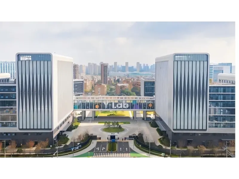
VETEK Semiconductor has established two major R&D platforms:
· Corporate R&D Center
· Yongjiang Laboratory Thermal Field Materials Innovation Center
These two platforms jointly undertake the research and development of advanced materials, process optimization, and product industrialization, providing continuous technological support for the company's long-term development.
The company continues to make breakthroughs in the following core technologies:
· Independent development of CVD equipment
· CVD SiC process optimization
· CVD TaC deposition technology
· High-purity material purification technology
· Precision graphite machining technology
· Semiconductor thermal field design
· High-temperature material performance optimization
· New semiconductor material development
Key Message: VETEK Semiconductor has established a complete manufacturing workflow covering purification → precision machining → coating deposition → inspection → packaging and shipment. The company operates an approximately 100-acre manufacturing base, more than 50 production lines, and 17 CVD SiC coating systems, with a maximum coating size of 1.5 meters.
|
Manufacturing Capability |
Specifications |
|
Manufacturing Base |
Approximately 100 acres |
|
Production Lines |
50+ |
|
CVD SiC Coating Systems |
17 units |
|
CVD TaC Coating Systems |
8 units |
|
Solid SiC Production Systems |
3 units |
|
Maximum Coating Size |
1.5 meters |
|
Annual Capacity for Large Susceptors (600 mm and above) |
Over 10,000 pieces |
· Ultra-precision CNC machining centers
· CNC machining centers
· CNC lathes
· CNC grinding machines
· Large horizontal machining centers
· High-precision inspection equipment
· High-purity purification systems
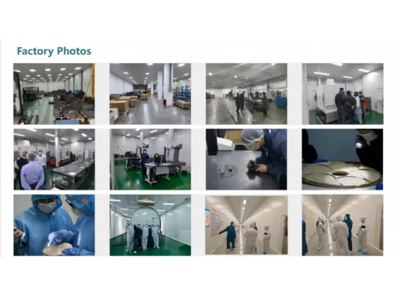
A new manufacturing base is currently under construction and will further expand the company's production capacity to meet growing global demand.
Key Message: VETEK Semiconductor has established a comprehensive quality management system covering the entire manufacturing process. High-purity materials can achieve a purity level of 6N–7N, while the batch-to-batch thickness consistency of CVD SiC coatings is controlled within ±10 μm. The company also provides complete material certifications and inspection documentation to support customer quality requirements.
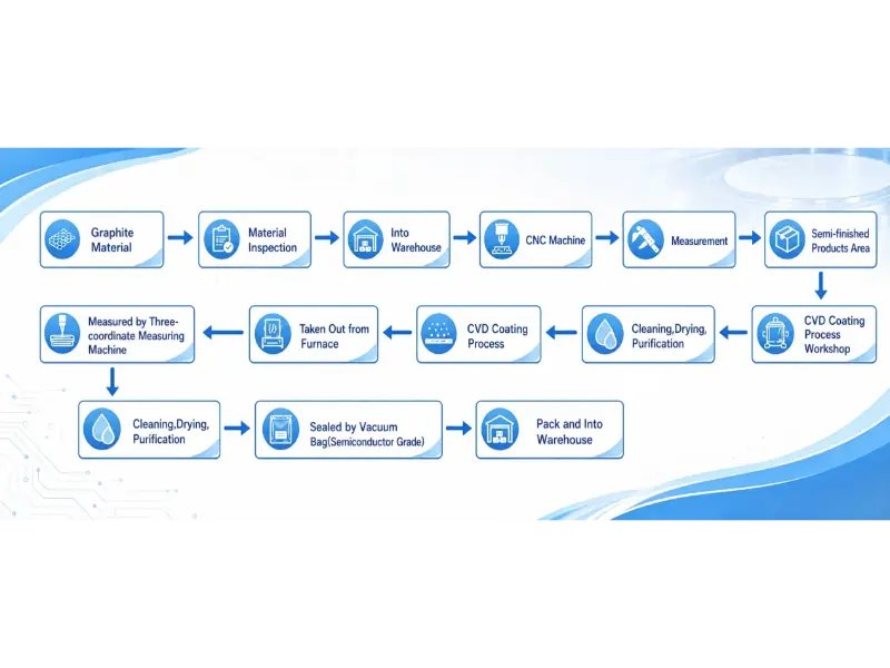
Semiconductor manufacturing places extremely stringent requirements on material purity, dimensional accuracy, and product consistency. VETEK Semiconductor has established a comprehensive quality management system covering every stage of production. Each product undergoes the following manufacturing process:
Raw Material Inspection → High-Purity Purification → Precision Machining → CVD Coating Deposition → Product Inspection → Final Inspection
· After deep purification, the purity of high-purity materials can be controlled at the 6N–7N level.
· Batch-to-batch coating thickness consistency for CVD SiC coatings is controlled within ±10 μm.
· For TaC-coated products, strict quality control is implemented for coating adhesion, surface integrity, and crack/pinhole inspection.
The company provides complete technical documentation, including:
· Material Certificate
· Certificate of Conformity (COC)
· Inspection Report
· Dimensional Inspection Report
· Coating Thickness Inspection Report
· Material Datasheet
· SDS/MSDS (where applicable)
· Packing List
· Commercial Invoice
· Certificate of Origin (according to export requirements)
Key Message: VETEK Semiconductor supports OEM/ODM services, custom manufacturing, sample orders, and small-volume production. Standard products typically have a lead time of 2–4 weeks, while global logistics are supported through DHL, FedEx, UPS, and ocean freight.
The company provides long-term services including:
· Manufacturing based on customer drawings
· Manufacturing based on supplied samples
· Reverse engineering
· Custom dimension design
· Graphite material substitution recommendations
· Coating solution optimization
· Thermal field structure optimization
· Complete thermal field component development
We support products ranging from 2-inch, 4-inch, 6-inch, and 8-inch platforms to even larger customized sizes.
Sample orders and small-volume production are available, enabling customers to carry out:
· Equipment validation
· Process qualification
· New product development
For volume production, stable supply plans can be established based on customers' annual purchasing forecasts.
|
Product Type |
Standard Lead Time |
|
Standard Products |
2–4 Weeks |
|
Standard Customized Products |
4–6 Weeks |
|
Complex Customized Products |
6–10 Weeks |
Long-term partners may establish safety stock programs to further improve delivery stability.
We support multiple international shipping methods, including:
· DHL
· FedEx
· UPS
· TNT (for samples and small-volume shipments)
· Air Freight (for urgent large-volume shipments)
· Ocean Freight (for large components and long-term bulk orders)
Supported trade terms include:
· EXW
· FOB
· FCA
· CIF
· DDP (available for selected countries)
Products are protected using multi-layer packaging, including:
· Cleanroom cleaning
· PE protective film
· Vacuum sealing
· Anti-static packaging
· Pearl cotton (EPE) cushioning
· Customized wooden crates
If any issues occur during transportation, including:
· Damaged packaging
· Shipping damage
· Quantity discrepancies
· Incorrect product models
customers may contact our sales team immediately. We will provide prompt support, including:
· Replacement shipments
· Product replacement
· Technical analysis
· Logistics claim assistance
to ensure customer satisfaction.
Pre-sales Support
· Product selection consultation
· Design for Manufacturability (DFM) analysis
· Material substitution recommendations
· Thermal field optimization suggestions
· Sample support
· Rapid quotation
After-sales Support
· Installation guidance
· Product usage recommendations
· Maintenance guidance
· Process optimization support
· Product lifetime analysis
· Failure analysis
· Rapid response to quality-related issues
Key Message: VETEK Semiconductor's products are widely used in five major industries, including semiconductor manufacturing, third-generation semiconductors, LED, new energy, and scientific research & advanced manufacturing.
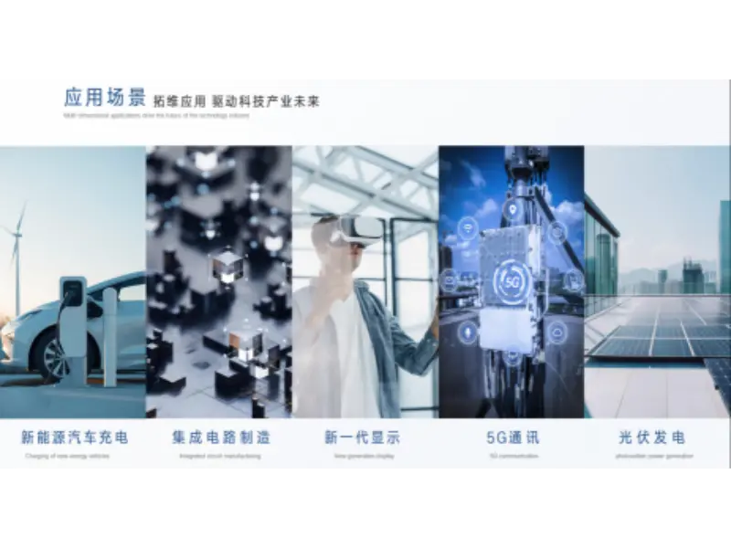
Semiconductor Manufacturing
· Integrated Circuits (IC)
· Power Semiconductors
· MEMS
· Compound Semiconductors
Third-Generation Semiconductors
· SiC Power Devices
· GaN Power Devices
· RF Devices
· Micro LED
LED Industry
· Blue LEDs
· Deep Ultraviolet LEDs (UV LEDs)
· Mini LEDs
· Micro LEDs
New Energy Industry
· New Energy Vehicles (NEVs)
· Photovoltaic Equipment
· Energy Storage Systems
Scientific Research and Advanced Manufacturing
· University Laboratories
· National Research Institutes
· Advanced Materials R&D Platforms
A: VETEK Semiconductor offers six major product categories, including CVD SiC coatings, CVD TaC coatings, Solid Silicon Carbide (Solid SiC), high-purity graphite and carbon-based materials, quartz and advanced ceramics, and semiconductor wafers, covering critical semiconductor processes such as epitaxy, etching, and crystal growth.
A: Through our deep purification process, the purity of high-purity materials can be controlled at the 6N–7N level. In addition, the batch-to-batch coating thickness consistency of our CVD SiC coatings is controlled within ±10 μm, ensuring stable performance during long-term high-temperature operation.
A: Yes. We accept sample orders and can provide single-piece or small-batch deliveries depending on the product type, allowing customers to conduct equipment validation, process qualification, and new product development.
A: The standard lead time is:
· Standard products: 2–4 weeks
· Standard customized products: 4–6 weeks
· Complex customized products: 6–10 weeks
For long-term customers, safety stock programs can also be established to further improve delivery stability.
A: Yes. We provide manufacturing based on customer drawings, manufacturing from supplied samples, reverse engineering, custom dimension design, material substitution recommendations, coating solution optimization, thermal field structure optimization, and complete thermal field component development services. We support products from 2-inch to 8-inch platforms, as well as larger customized sizes.
A: Our products are widely used in LPE, Aixtron, Veeco, ASM, and other mainstream epitaxy systems, as well as etching equipment, oxidation/diffusion furnaces, crystal growth furnaces, and other semiconductor processing equipment. They are suitable for critical manufacturing processes including:
· Silicon Epitaxy
· SiC Epitaxy
· GaN Epitaxy
· LED Epitaxy
· Plasma Etching
· Diffusion
· Oxidation
· Annealing
· Rapid Thermal Processing (RTP)
A: VETEK Semiconductor has established a complete quality management system covering the entire manufacturing process:
Raw Material Inspection → High-Purity Purification → Precision Machining → CVD Coating Deposition → Product Inspection → Final Inspection
Every product undergoes multiple inspections, including:
· Visual inspection
· Dimensional inspection
· Coating thickness measurement
· Flatness inspection
· Concentricity inspection
· Coating uniformity inspection
Complete quality traceability records are maintained throughout the manufacturing process.
A: VETEK Semiconductor has been recognized as a National Specialized and Sophisticated "Little Giant" Enterprise. The company's founder, Dr. He Shaolong, has been selected as a leading talent under the Zhejiang Province "Ten Thousand Talents Program." Our products have entered the core supply chains of numerous publicly listed industry leaders, including Leon Microelectronics, Jiangfeng Electronics, HC Semitek, and Zhaochi Co., Ltd.
· National Specialized and Sophisticated "Little Giant" Enterprise, ranking among the first-tier suppliers in China's semiconductor epitaxy thermal field industry.
· Dual R&D Platforms: Corporate R&D Center + Yongjiang Laboratory Thermal Field Materials Innovation Center.
· Six Business Divisions and Six Major Product Categories, providing comprehensive coverage of semiconductor high-temperature thermal field applications.
· Fully Integrated Manufacturing Chain: Complete in-house manufacturing system covering purification → precision machining → CVD coating → inspection, ensuring full process control.
· Trusted by More Than 30 Semiconductor Industry Customers, with products entering the core supply chains of multiple leading publicly listed semiconductor companies.
· OEM/ODM and Custom Manufacturing Supported, providing flexible solutions tailored to customer requirements.
· Sample Orders and Small-Batch Production Available, helping customers reduce validation costs and accelerate product development.
· Comprehensive Quality Control and Full Product Traceability, ensuring long-term product stability and consistent performance.
· Global Logistics Network and Comprehensive Pre-sales & After-sales Support, providing reliable service for customers worldwide.
Driven by continuous technological innovation, VETEK Semiconductor has established a complete service ecosystem spanning research and development, manufacturing, and global delivery, centered around critical semiconductor manufacturing processes.
From high-purity materials to precision semiconductor components, and from advanced coating technologies to complete thermal field solutions, the company is committed to providing high-performance, reliable, and sustainable key materials and core components for the global integrated circuit, third-generation semiconductor, LED, photovoltaic, and advanced manufacturing industries.
Looking ahead, VETEK Semiconductor will continue to uphold its commitment to quality excellence and technological innovation, working closely with customers worldwide to drive the advancement of next-generation semiconductor materials and technologies.

+86-579-87223657
Wangda Road, Ziyang Street, Wuyi County, Jinhua City, Zhejiang Province, China