




QR Code

Products
Contact Us


Fax
+86-579-87223657

Email

Address
Wangda Road, Ziyang Street, Wuyi County, Jinhua City, Zhejiang Province, China



● Purity (GDMS Verified): > 99.99995% (Up to 6N-7N) | Keeps the chamber free of trace metal risks.
● Structural Solidness: ≥3.21 g/cm3 | Reaches theoretical density; leaves no voids for outgassing or micro-particles to hide.
● Thermal Regulation: 200 - 300W/m·K | Spreads heat rapidly to keep wafer-rim temperatures perfectly even.
● Electrical Range: 0.01 - 10 Ωcm | Adaptable resistivity to steady the plasma sheath and refine RF connection.Surface Rigidity: ≥2500 HV | Resists abrasive wear during continuous dry-etching cycles.
● Advanced process plasma etching
● Thin film deposition processes (PECVD/ALD)
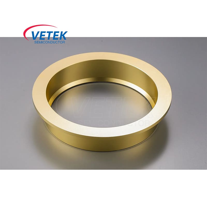
● Solid SiC etching rings are key consumables in advanced chip manufacturing, used to ensure the uniformity of wafer edge processes, improve yield and extend component life in plasma etching and deposition processes.
● Issue: Costly Idle Time from Fast Part Erosion
The Fix: Vetek’s CVD-grown structure shows an erosion pace 10 to 20 times slower than quartz and 3 to 5 times slower than bulk silicon. Fabs get longer production runs and far fewer emergency chamber vents.
● Issue: Edge Yield Collapse ("The Edge Effect")
The Fix: Slow, predictable wear across the ring face stops the plasma sheath from tilting over time. This preserves tight Critical Dimension (CD) limits right at the wafer perimeter.
● Issue: Defect Spikes from Sintered-Part Shedding
The Fix: Our gas-phase synthesis leaves behind zero grain-boundary binders or metallic fillers. Without these weak spots, the ring won't flake or cause micro-masking defects on the wafer surface.
● Tool Drop-In Integration: Custom-machined to match the strict spacing specs of global etcher brands like Lam, AMAT, and TEL.
● Resistivity Matching: We tune the electrical profile of each batch to line up perfectly with your specific recipe parameters.
● Advanced Finishes: Employs ultra-clean Chemical Mechanical Planarization (CMP) to smoothen rough surfaces, lowering particle counts during early tool seasoning.
● Intricate Form-Factors: We hold tight tolerances (±0.01mm) on tricky, multi-stepped edge rings and interlocking ring setups.
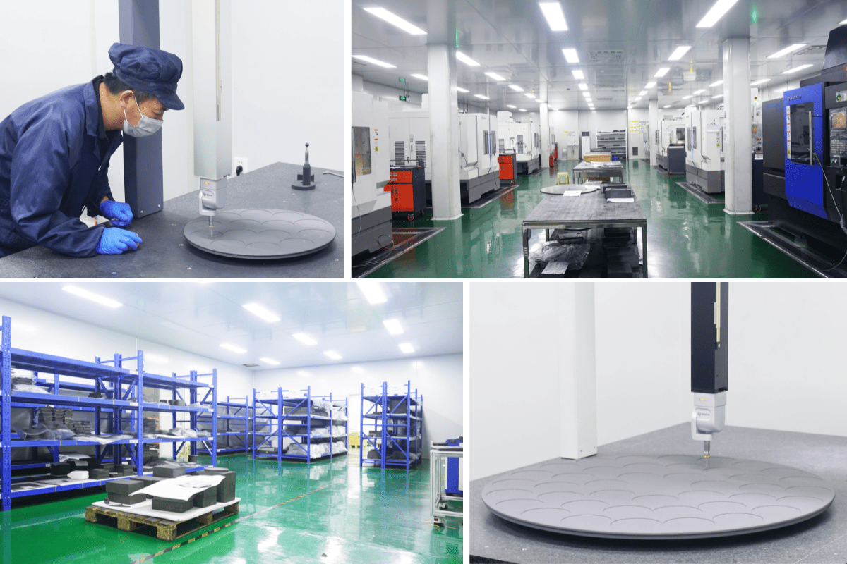
Vetek Semiconductor Warehouse:
Address
Wangda Road, Ziyang Street, Wuyi County, Jinhua City, Zhejiang Province, China
Tel
+86-579-87223657
Wangda Road, Ziyang Street, Wuyi County, Jinhua City, Zhejiang Province, China