

News

What Is Silicon Carbide Coating? CVD Process, Properties and Semiconductor Uses

2026-09-09 0 Leave me a message

Detail Summary

A silicon carbide coating (SiC coating) is a dense SiC layer deposited on a component surface, usually high-purity graphite, to create a chemically resistant and thermally stable process interface. In semiconductor equipment, the coating is commonly produced by chemical vapor deposition (CVD).

Its performance comes from the combined system of graphite substrate, CVD SiC layer, component geometry and reactor environment.

1. What Is a Silicon Carbide Coating?

Graphite is widely used for semiconductor hot-zone parts because it is machinable and thermally stable. However, bare graphite can react with process gases, oxidize, release impurities or generate particles as the surface degrades.

CVD SiC changes that surface condition. Silicon carbide is deposited as a dense polycrystalline layer over the machined graphite body, creating a barrier between graphite and the process environment.

Process Gas / Wafer → Dense CVD SiC Surface → SiC/Graphite Interface → High-Purity Graphite Body

Graphite supplies the structural body, thermal mass and machinability; SiC provides the process-facing surface. The interface must survive deposition, cooling and repeated reactor cycles.

SGL Carbon describes commercial SiC coatings as dense, wear- and corrosion-resistant CVD layers deposited on isostatic graphite, with applications spanning semiconductor crystal growth, silicon/SiC epitaxy and MOCVD.

This is why semiconductor-grade SiC-coated parts should be evaluated as engineered material systems, rather than simply as “graphite with a coating.”

2. Why Is Graphite Coated with SiC in Semiconductor Equipment?

The purpose is to combine graphite's manufacturing and thermal advantages with a surface better suited to demanding semiconductor conditions.

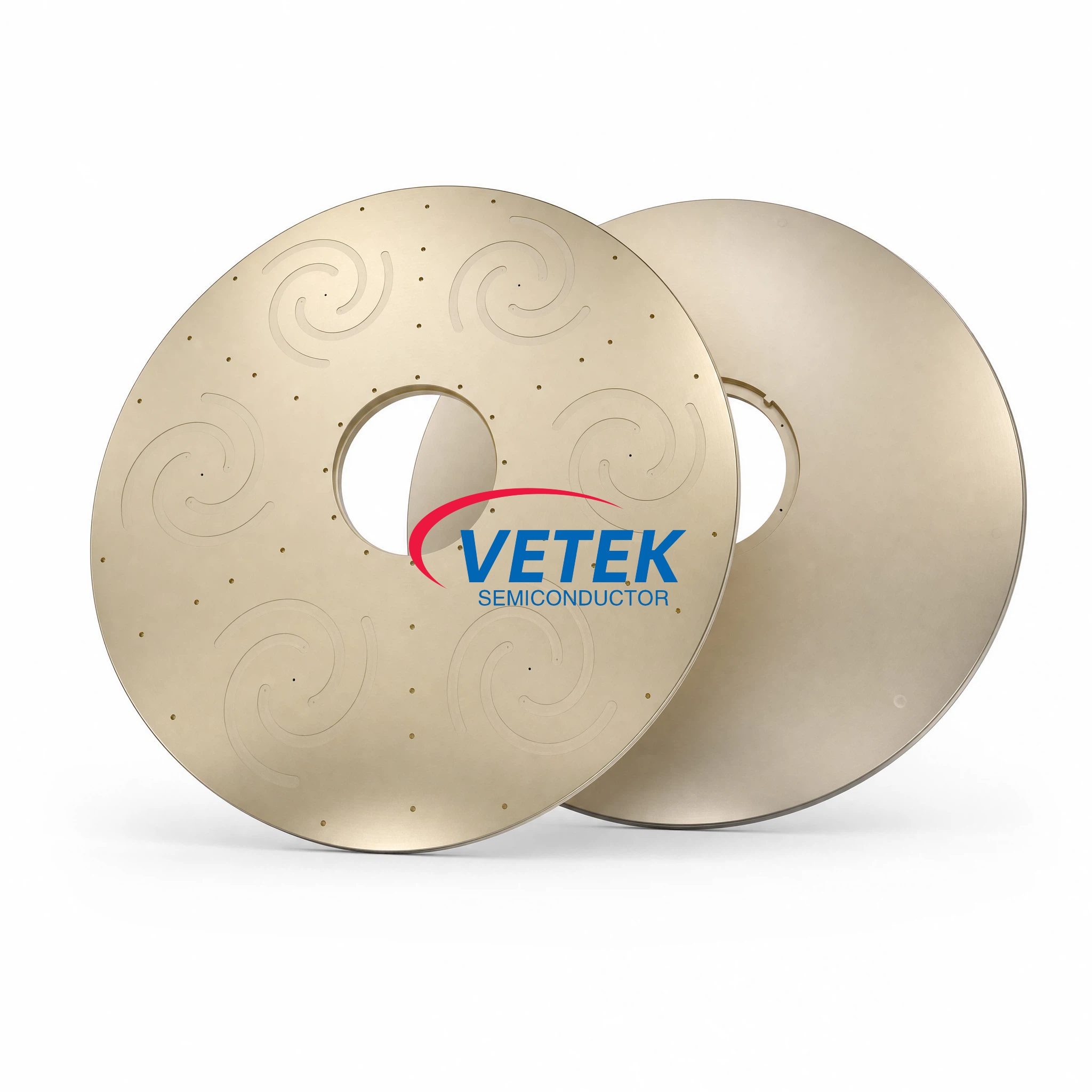
A graphite susceptor or wafer carrier can be machined to tight tolerances and complex pockets. CVD SiC then protects the surface exposed to process gases and cleaning. This combination addresses four major concerns.

Contamination control. A dense, high-purity surface helps isolate the underlying graphite from the wafer environment.

Chemical durability. Epitaxy and MOCVD use aggressive precursors and cleaning chemistry; SiC improves resistance compared with exposed graphite.

Particle control. Cracks, peeling or surface degradation can become particle sources, so coating integrity matters directly to process cleanliness.

Thermal repeatability. Susceptors and carriers are part of the reactor thermal field. Their geometry and surface condition must remain stable so wafer temperature remains repeatable.

Mersen identifies high temperature, high vacuum, aggressive gaseous precursors, contamination control and resistance to cleaning acids as key operating requirements for graphite equipment used in epitaxy and MOCVD. It also highlights graphite/SiC CTE compatibility as important to coating integrity. 

This explains why coating quality cannot be separated from graphite quality, dimensional accuracy or reactor conditions. A chemically excellent SiC layer on a distorted or poorly designed component may still deliver poor process performance.

3. How Is CVD Silicon Carbide Coating Produced?

A typical manufacturing chain is:

Graphite Selection → Precision Machining → Purification → Surface Preparation → CVD SiC Deposition → Inspection

The graphite is selected for purity, microstructure and thermal behavior, then machined before coating because flatness, pocket depth and edge geometry affect final dimensions and coating uniformity.

During CVD, gaseous precursors enter a high-temperature reactor. Reactive species reach the graphite surface, where SiC nucleates and grows into a continuous layer.

SGL Carbon publicly reports typical SiC deposition temperatures of approximately 1,200–1,300°C for its commercial coating process. It reports β-SiC, or cubic 3C-SiC, for one coating system.

Recent research on CVD-SiC-coated graphite susceptors further demonstrates that the coating structure depends strongly on processing conditions.

A 2026 Scientific Reports study investigated deposition from 1,100 to 1,350°C, together with changes in pressure and H₂/MTS ratio. The researchers observed significant changes in coating morphology, roughness, stoichiometry and hardness, demonstrating the relationship between:

CVD Parameters → SiC Microstructure → Coating Properties → Component Performance

The important engineering lesson is that “CVD SiC” is not one fixed material.

A specification such as:

“100 μm SiC coating”

describes only thickness.

It does not fully define:

l purity;

l porosity;

l grain structure;

l surface roughness;

l coating uniformity;

l interface quality;

l residual stress.

For semiconductor equipment, those factors may be as important as nominal thickness.

4. Which SiC Coating Properties Matter Most?

For semiconductor use, the most useful properties are those connected to contamination control, process stability and component lifetime.

Property

Engineering Importance

Purity

Limits contamination at the process surface

Density / Porosity

Controls barrier integrity

Thickness

Affects protection, dimensions and stress

Thickness Uniformity

Matters across pockets, edges and complex geometry

Surface Roughness

Influences deposits, cleaning and particles

CTE

Controls thermal mismatch with graphite

Hardness

Supports wear resistance

Grain Structure

Reflects deposition conditions

Chemical Resistance

Protects graphite from reactive gases

Thermal Stability

Supports repeated high-temperature cycling

As a public commercial benchmark, SGL Carbon reports for one SiC coating a bulk density of approximately 3.2 g/cm³, hardness of 40 GPa, thermal expansion of 4.3 × 10^-6 K^-1 from 100–600°C and a typical coating thickness of 100 μm. These values are examples rather than universal semiconductor specifications.

Two parameters deserve particular attention: coating thickness and CTE.

1. A thicker SiC coating is not automatically better.

Additional thickness may provide a larger protective barrier, but it may also alter component dimensions and increase accumulated residual stress. This becomes important for susceptors and wafer carriers where pocket depth, flatness and edge geometry are process-critical.

2. CTE matching is equally important.

SiC is deposited at high temperature and then cools together with the graphite substrate. If SiC and graphite expand and contract differently, mechanical stress develops near the interface.

A simplified failure path is:

CTE Mismatch → Residual Stress → Microcrack → Crack Propagation → Delamination → Particles / Exposed Graphite

This mechanism explains why coating failure cannot always be solved simply by increasing thickness.

A 2026 Ceramics International study specifically investigated SiC deposited on graphite at 1,260°C, 1,280°C and 1,320°C and found that deposition temperature affected microstructure and interfacial adhesion.

Therefore, coating quality should be judged by the combination of:

Purity + Microstructure + Uniformity + Interface Integrity + Geometry

rather than thickness alone.

5. Where Is SiC-Coated Graphite Used, and How Should It Be Selected?

The strongest applications are components that face high temperature, reactive chemistry and strict wafer-level requirements.

1. Silicon Epitaxy

SiC-coated graphite susceptors support wafers while participating in heat transfer. Flatness, pocket geometry, coating uniformity and surface condition can influence wafer temperature and epitaxial uniformity.

The coating is therefore part of a wider thermal system:

Heater / Energy Source → Susceptor → Wafer Thermal Boundary → Wafer Temperature → Epitaxial Growth

2. Silicon Carbide Epitaxy

SiC epitaxy places particularly demanding requirements on thermal-field materials. Susceptors, rings and related components must maintain chemical stability, low contamination and dimensional consistency through repeated high-temperature operation.

3. GaN and LED MOCVD

MOCVD wafer carriers and satellite platforms operate in precursor-rich environments where carrier temperature distribution influences growth conditions across the wafer.

Changes in carrier geometry or surface condition may contribute to variations in:

l wafer temperature;

l growth rate;

l film thickness;

l composition;

l wafer-to-wafer uniformity.

Mersen specifically identifies high-purity SiC-coated graphite, uniform thermal behavior, resistance to aggressive gases and durability against in-situ chemical cleaning as important requirements for epitaxy applications.

4. Other High-Temperature Processes

Selected RTP/RTA, CVD, ALD and other thermal-field components may also use SiC-coated graphite when temperature, chemistry, contamination risk and geometry justify it.

Selection should begin with the reactor and process, not a generic coating specification.

Define:

l process and reactor model;

l wafer size;

l operating temperature;

l process and cleaning gases;

l component drawing;

l graphite requirement;

l critical dimensions and flatness;

l coating thickness;

l surface roughness;

l inspection requirements.

The most useful RFQ asks one central question:

What must this component do inside the reactor?

The SiC coating can then be engineered around the actual objective rather than an isolated material parameter.

For epitaxy and MOCVD, the goal is not simply the longest-lasting coating. It is a component capable of supporting:

Stable Wafer Temperature + Low Contamination + Low Particle Generation + Repeatable Growth + Predictable Service Life

6. FAQ

1. What is the main purpose of silicon carbide coating on graphite?

It creates a high-purity, chemically resistant process surface while retaining the machinability and thermal advantages of the graphite body.

2. Why is CVD used for SiC coating?

CVD allows SiC to grow directly on complex graphite surfaces and provides control over coating structure, thickness and uniformity when the deposition process is properly engineered.

3. Is thicker SiC coating always better?

No. Thickness must be balanced against residual stress, dimensional tolerance, component geometry and service conditions.

4. What causes SiC coating to crack or delaminate?

Common contributors include graphite/SiC CTE mismatch, residual stress, interface defects, inappropriate deposition conditions and repeated thermal cycling.

5. What information is needed for a SiC-coated graphite RFQ?

Provide the drawing, reactor model, process, wafer size, operating temperature, process and cleaning gases, graphite requirement, coating specification, critical tolerances, inspection criteria and quantity.


References

1. SGL Carbon. SIGRAFINE® SiC Coatings. Technical data and application information for CVD SiC coatings on isostatic graphite.

2. Mersen. Semiconductor Process Equipment — Ultra-Pure Graphite Coated with Silicon Carbide. Technical information for epitaxy and MOCVD applications.

3. Huo, Y., Qin, S., Chen, Y., et al. “Study of the process-structure-property correlation in CVD-SiC coatings on graphite substrates.” Scientific Reports, Vol. 16, Article 4150, 2026.

4. Ma, Q., et al. “Interfacial adhesion of CVD-SiC coatings on graphite substrates: Role of temperature in microstructure and mechanical properties.” Ceramics International, Vol. 52, Issue 3, 2026, pp. 3711–3718.

Related News
Leave me a message
X
We use cookies to offer you a better browsing experience, analyze site traffic and personalize content. By using this site, you agree to our use of cookies.Privacy Policy