


QR Code

Products
Contact Us


Fax
+86-579-87223657

Email

Address
Wangda Road, Ziyang Street, Wuyi County, Jinhua City, Zhejiang Province, China



To truly understand how an advanced chip achieves high-speed computation and high-power output, we must delve into the two fundamental pillars of its physical structure—the semiconductor substrate and the epitaxial growth process.
Simply put, the substrate provides the “foundation” for mechanical support and heat dissipation, while the epitaxial layer is the “active functional layer” meticulously built upon that “foundation.” Although the two terms differ by only one character, they have fundamental differences in material structure, fabrication processes, and functional roles. This article will systematically outline their technical differences, key parameters, and decisive impact on the final device’s performance.
[Key Conclusion of This Section]: A semiconductor substrate serves as the device’s “skeleton” and “heat sink.” High-purity single-crystal silicon (Si) dominates the consumer market, while silicon carbide (SiC), with its high thermal conductivity of 4.9 W/cm·K, has become an indispensable choice for electric vehicles and high-voltage applications.
Semiconductor substrates form the structural and thermal foundation of nearly all semiconductor devices. From a mechanical perspective, they serve as the physical platform supporting micro- and nanostructures; more importantly, they provide a continuous crystal lattice template that determines the crystal orientation and structural integrity of subsequently deposited layers.
Depending on application requirements, substrate materials can be single-crystal, polycrystalline, or even amorphous; however, high-performance electronic devices rely almost entirely on high-purity single-crystal ingots to minimize grain boundaries and defects that hinder carrier mobility.
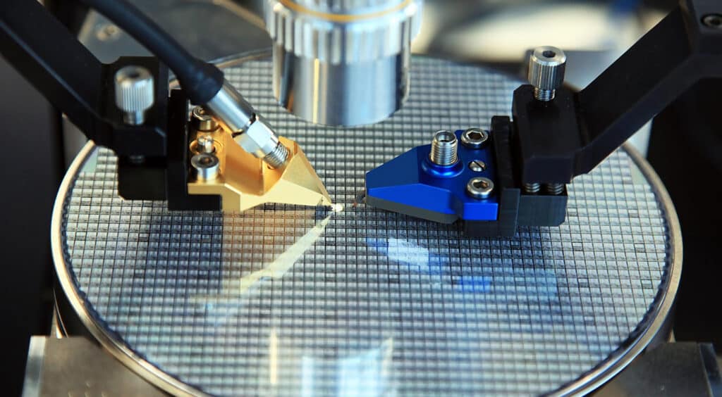
The choice of large-size substrates directly impacts device performance, manufacturing yield, and cost structure. The industry primarily uses three major types of substrates:
During actual device operation, bulk substrates perform two irreplaceable key functions:
Mechanical Support: Provides structural rigidity during severe thermal cycling, high-vacuum chemical processes, wafer handling, and back-end packaging, effectively preventing wafer warping and fracture.
Heat Conduction (Heat Dissipation): Modern chips generate massive localized heat fluxes; bulk silicon substrates act as direct heat sinks, dissipating heat outward to prevent overheating of the junction region and thermal runaway.
[Key Conclusion of This Section]: The epitaxial layer is the “soul of a chip’s performance.” CVD/MOCVD handle large-scale industrial production, while MBE (Molecular Beam Epitaxy) enables ultra-steep interfaces with atomic-level precision. Without epitaxial technology, the ultra-low on-resistance of 5G millimeter-wave radar and high-voltage MOSFETs would be impossible.
Although the substrate provides a stable foundation, bulk-grown single crystals inevitably contain microdefects, natural impurities, and fixed electrical characteristics. To fabricate ultra-high-speed, high-efficiency devices, manufacturers have adopted epitaxy—the controlled deposition of ultra-clean, thin crystal layers onto a target substrate.
During the epitaxial process, atoms from vapor or molecular beams are deposited onto the heated substrate surface and are perfectly aligned with the underlying crystal lattice. The resulting epitaxial wafer exhibits extremely high crystal purity, with a defect density several orders of magnitude lower than that of the bulk substrate.
Modern epitaxial growth is primarily achieved through the following advanced methods:
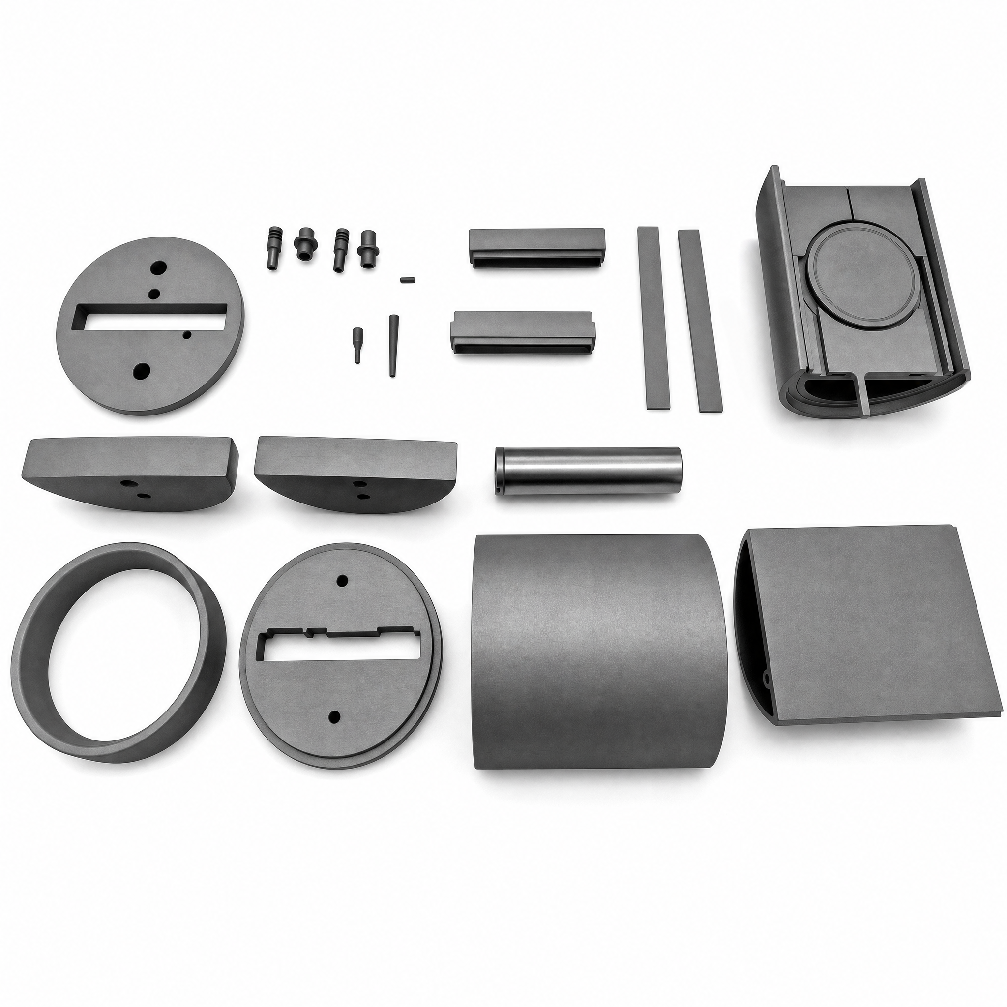
High-quality epitaxial deposition relies not only on precise process control but also on the lifespan management of key components inside the reaction chamber (such as SiC-coated graphite substrates), which directly impacts process stability and yield.
Epitaxy enables device architectures that cannot be achieved with bulk materials alone:
For the definition of the semiconductor epitaxy process, refer to: What is semiconductor epitaxy process?
[Key Conclusion of This Section]: The most direct way to distinguish between the two is to examine their “functional roles”—the substrate is responsible for withstanding physical and thermal shocks, while the epitaxial layer is responsible for withstanding current and electric fields. By decoupling the active region from the defect-prone region, epitaxial wafers achieve leakage current levels more than one order of magnitude lower than devices fabricated directly on a substrate.
For a visual comparison, the table below summarizes the fundamental differences between bulk substrates and epitaxial wafers in terms of key manufacturing parameters:
|
Deposition Method |
Key Mechanics & Precursors |
Main Advantages |
|
Chemical Vapor Deposition (CVD) |
High-temperature reaction of gas precursors at 1100–1400°C. |
Ultra-high purity (>99.999%), 100% theoretical density, strong chemical bonding. |
|
Physical Vapor Deposition (PVD) |
Magnetron sputtering or electron-beam evaporation under ultra-high vacuum conditions. |
Low process temperature, precise nanoscale thickness control, excellent optical-grade density. |
|
Thermal Spraying Techniques |
Plasma or high-velocity oxy- fuel (HVOF) spraying of melted/semi-melted SiC micro-powders. |
High deposition rate, cost-effective for large-area structural components. |
|
Electrochemical Deposition |
Electro-crystallization of silicon/carbon precursors from molten salt or organic liquid solutions. |
Non-line-of-sight coating on complex conductive substrates, low temperature requirement. |
|
Slurry Coating & Sintering |
Dip/spray liquid slurry containing SiC powders and organic binders, followed by high-temperature sintering. |
Simple equipment requirement, low operational cost, suitable for thick protective coatings. |
[Key Conclusion of This Section]: Natural microdefects and thermal stress points in bulk substrates are the “hidden killers” that cause high leakage current and low breakdown voltage in devices. The essence of epitaxial technology lies in decoupling the “defective mechanical substrate” from the “defect-free active functional layer,” thereby isolating carrier transport within the pure epitaxial layer. This decoupling design directly results in higher operating frequencies, lower power consumption, and longer device lifetimes—a qualitative leap that can never be achieved by using bulk substrates alone.
The introduction of epitaxial technology is not merely “adding a layer of film,” but rather a qualitative leap in device reliability and electrical performance.
Even with the highest chemical purity, standard bulk substrates inevitably contain microporosity, oxygen precipitates, and thermal stress points left over from the crystal pulling process. Fabricating devices directly on bulk substrates often results in high leakage current and low breakdown voltage tolerance.
In contrast, epitaxial wafers isolate carrier transport within a pure, defect-free epitaxial layer. By decoupling the active functional region from the defect-prone mechanical substrate, manufacturers are able to achieve:
For example, in the field of power semiconductors, the quality of the SiC homogeneous epitaxial layer directly determines the breakdown voltage rating and on-resistance of MOSFET devices—something that bulk SiC substrates cannot achieve on their own.
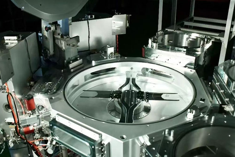
(The following questions are derived from common technical challenges encountered by semiconductor production line process engineers during actual epitaxial growth processes)
Q1: If particulate matter suddenly increases during epitaxial growth, aside from chamber leaks, what other easily overlooked areas should be investigated?
A: This is one of the most challenging unexpected situations engineers face during routine wafer runs. After confirming that the chamber is airtight, we recommend prioritizing the investigation of three “hidden corners”:
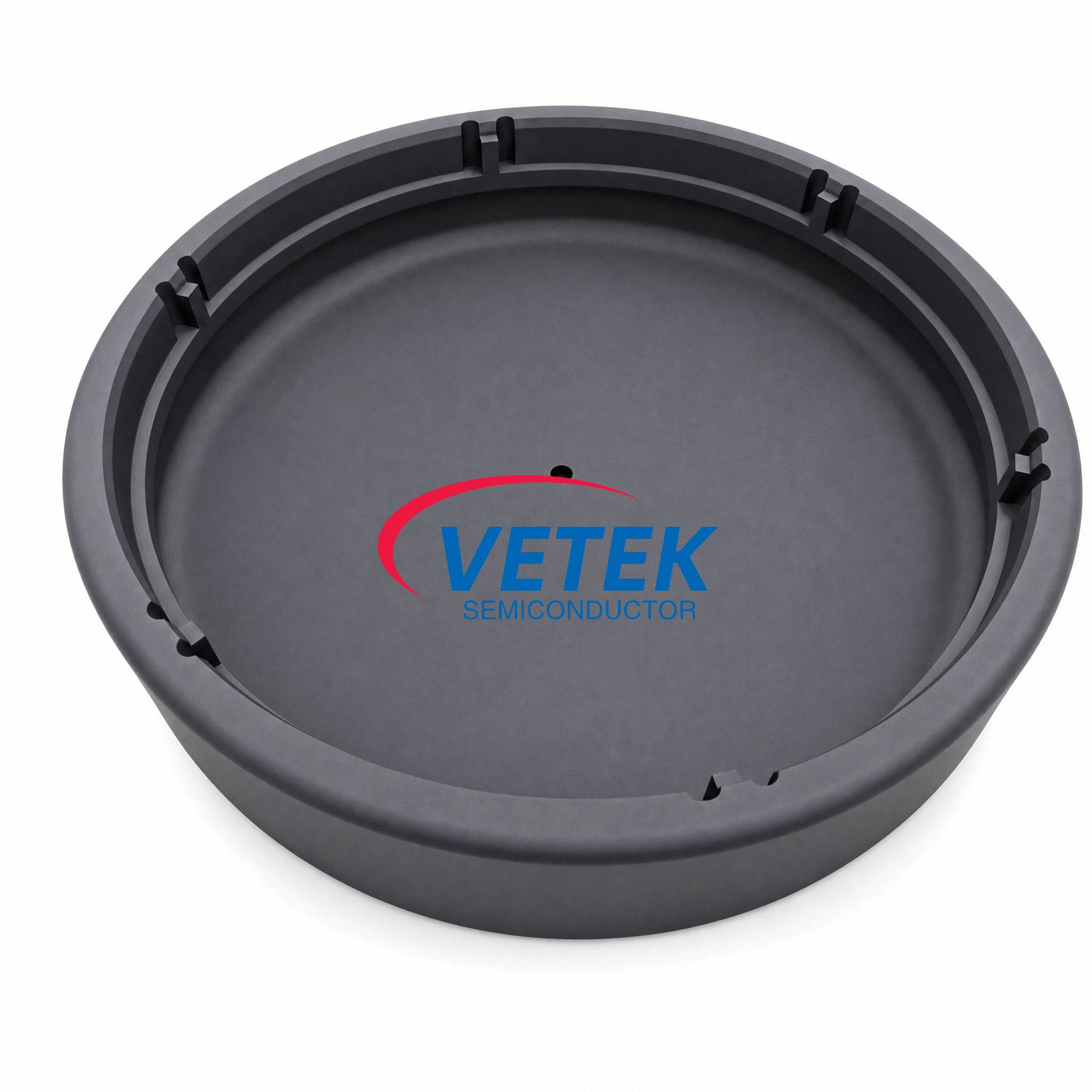
1. Surface condition of the graphite susceptor: Microcracks or peeling areas in the SiC coating can release particles at high temperatures. If the susceptor has been used for more than 1000 runs, we recommend replacing it immediately for testing—many particle issues disappear after replacing the susceptor with one that has an intact coating.
2. Pressure transients during gas line switching: In MOCVD systems, pressure fluctuations at the moment of source gas switching may cause byproducts to detach from the inner walls of the piping. We recommend inspecting the response curve of the automatic pressure controller (APC) to confirm whether pressure overshoot is occurring.
3. Contaminants on the substrate’s backside: If there is fine dust or organic residue on the backside of the substrate before it enters the chamber, it may “migrate” to the front-side epitaxial layer at high temperatures—this is the most commonly overlooked issue.
Particle troubleshooting is essentially a process of “elimination”: Start with the most frequently replaced consumables and trace the issue step by step toward the deeper parts of the chamber.
Q2: In SiC epitaxy, how narrow is the process window for step-flow growth? What are the tolerances for temperature and pressure deviations?
A: This question touches on the core of the SiC epitaxy process—step-flow growth requires three conditions to be met simultaneously within an extremely narrow window: sufficient surface mobility, an appropriate nucleation barrier at the step edge, and suppression of three-dimensional island growth.
Based on practical data from mass production lines:
In practical engineering applications, most process engineers prefer to first fix the temperature and then fine-tune the pressure to find the window—because the chamber responds more quickly to pressure changes, making it suitable for rapid DOE (Design of Experiments) scans.
Q3: How is the replacement cycle for the graphite susceptor in MOCVD equipment determined? Is it based on the number of runs or visual inspection?
A: This issue directly relates to the balance between process yield and production costs and is a key focus for both production line engineers and procurement decision-makers.
The industry-standard practice is a dual-track approach combining “batch lifespan” and “visual inspection”:
①Visible peeling or cracking of the coating;
② Discolored patches with a diameter >1 mm on the surface (indicating coating damage and oxidation of the graphite substrate);
③ Recurring localized thickness variations in the epitaxial layer, provided that airflow distribution factors have been ruled out.
A widely validated engineering practice is to set the replacement cycle at 80% of the supplier’s recommended lifespan, while simultaneously establishing a substrate lifespan database by photographing and archiving the appearance of each batch—this approach avoids both premature scrapping (which causes waste) and gambling until the very last furnace, which could result in batch-wide scrap.
Q4: When epitaxial wafer bow or warp exceeds specifications, is this primarily due to the substrate or the epitaxial process?
A: This is the most hotly debated “attribution of responsibility” issue among engineers during yield analysis meetings. The answer is—both contribute, but the relative weight varies depending on the material system:
A pragmatic troubleshooting sequence for warpage issues: First, verify the substrate’s incoming warpage data (supplier Cpk report) → Then, check the epitaxial furnace’s temperature uniformity (thermocouple calibration) → Finally, adjust the process recipe.
In summary, the substrate serves as the “skeleton and heat sink,” while the epitaxial layer acts as the “brain and muscles.” Both are indispensable:
If you are focused on cost-sensitive standard logic chips or simple discrete devices, high-quality, large-size silicon substrates are sufficient to meet your needs.
If your application involves high-frequency communications, high-voltage power conversion, or high-sensitivity photodetection, then wafers produced using precision epitaxial processes are your best choice.
In today’s semiconductor manufacturing industry, which continually pursues “faster, smaller, and more efficient” solutions, epitaxial technology has become a core tool for breaking through the physical limits of Moore’s Law.
Need custom epitaxial wafers for your project or want to learn about specific substrate selection options?
[Click here to contact us] or call [+86-18069220752], and our process engineers will provide you with professional technical support.
+86-579-87223657
Wangda Road, Ziyang Street, Wuyi County, Jinhua City, Zhejiang Province, China