




QR Code

Products
Contact Us


Fax
+86-579-87223657

E-mail

Address
Wangda Road, Ziyang Street, Wuyi County, Jinhua City, Zhejiang Province, China



|
Industry |
Semiconductor Manufacturing, Technical Ceramics, Third-Generation Semiconductors (GaN/SiC Epitaxy) |
|
Process |
CVD Silicon Carbide Deposition, MOCVD Epitaxial Growth, Interface Stress Control |
|
Solution |
Customized High-Purity Graphite Susceptor + Precision CVD Silicon Carbide (SiC) Coated Components |
|
Services |
CVD Process Diagnosis, Thermal & Flow Field Optimization, Engineering Design, Manufacturing & Quality Documentation |
|
Results |
• Comprehensive coating yield achieved a leapfrog increase from 50% to 90% |
|
Embedded Links |
Related Products: CVD Silicon Carbide Coated Graphite Susceptor | High-Purity Semiconductor Graphite Parts |
During the epitaxial growth process of compound semiconductors and third-generation semiconductors, the high-purity graphite susceptors and graphite parts inside MOCVD equipment must withstand high temperatures and severe chemical corrosion, relying heavily on dense CVD silicon carbide (SiC) coatings for protection. Addressing the customer's challenge of silicon carbide coating edge yellowing and reduced adhesion inside high-temperature reaction chambers, VeTek Semiconductor completely eliminated edge defects through deposition kinetics reconstruction and process parameter control, driving the finished product yield up from 50% to 90%, significantly reducing customer equipment downtime and component replacement costs.
|
Core Conclusion: Edge yellowing of MOCVD high-purity graphite silicon carbide coating is a typical manifestation of micro-stress and segregation. Through phased deposition rate control and flow field optimization, a leapfrog improvement in coating yield from 50% to 90% can be achieved. |
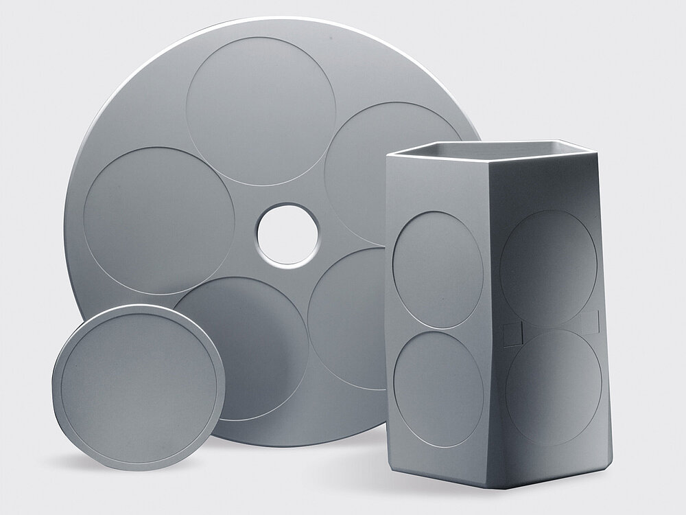
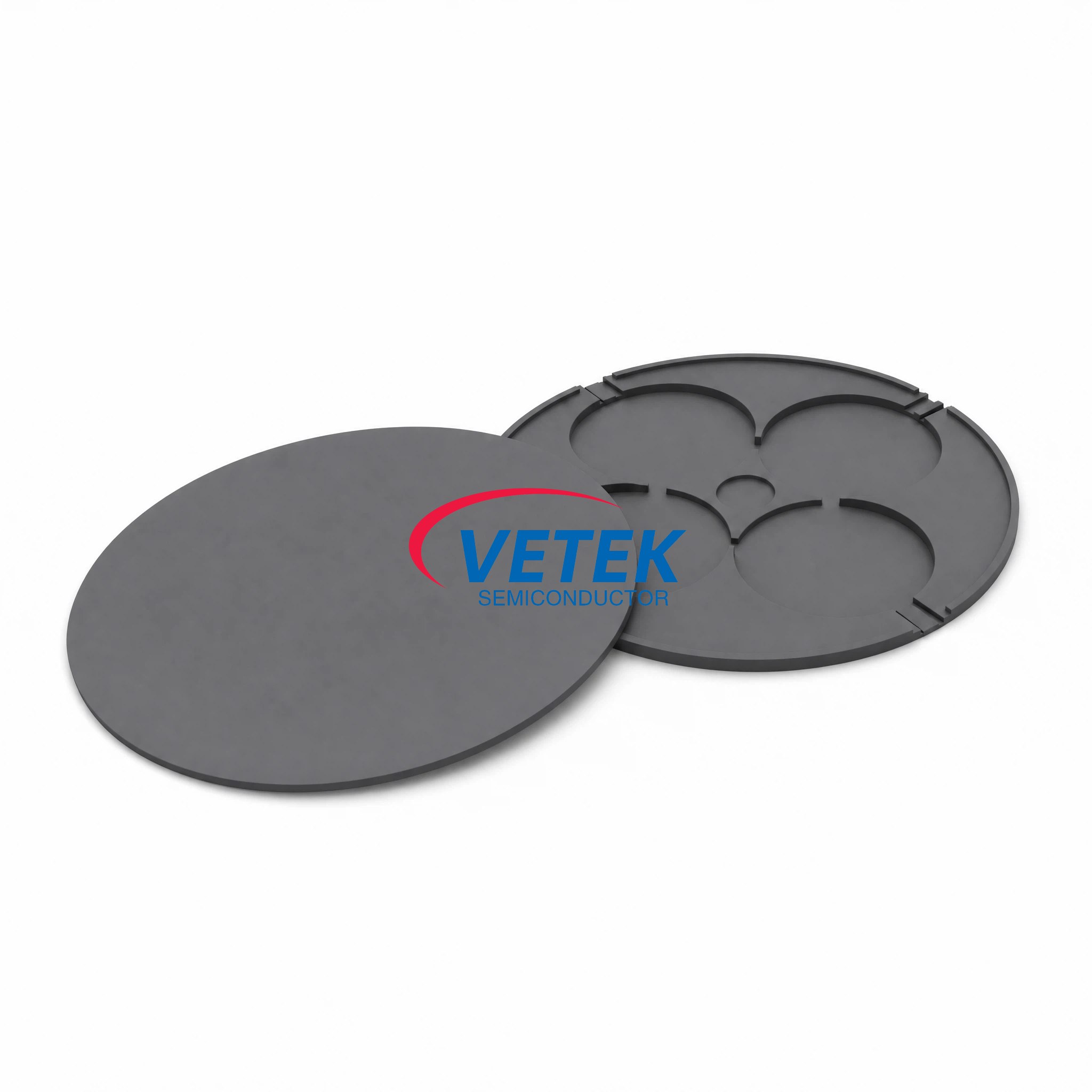
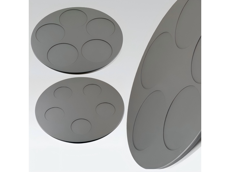
[Figure 1: MOCVD Silicon Carbide Coated Graphite Susceptor]
During the epitaxial growth of compound semiconductors and third-generation semiconductors, the quality of CVD silicon carbide coating on graphite susceptors and thermal field components directly determines wafer quality and production cost. Below is the comparison of key metrics before and after process optimization by VeTek Semiconductor:
|
Evaluation Dimension |
Before Improvement (Original Process Status) |
After Improvement (VeTek Optimization Scheme) |
|
Core Defect Morphology |
Explicit yellowing at coating edges, relatively high microscopic porosity |
Uniform color appearance across surface, no edge yellowing |
|
Initial Coating Deposition Rate |
25 μm/h (Rapid deposition leads to stress concentration) |
12 μm/h (Smooth transition, tight interface) |
|
Overall Production Yield |
50% (Severe scrap and rework present) |
90% (Stable batch delivery standard) |
|
Core Conclusion: Advanced compound semiconductor epitaxy demands almost rigorous crystallization quality and thermal conduction uniformity from CVD silicon carbide coated graphite components. |
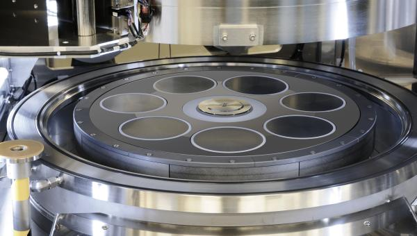
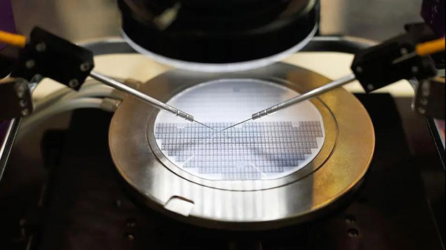
[Figure 2: Working Scene of Graphite Susceptor and Wafer Tray Inside MOCVD Reaction Chamber]
The partner in this project is a third-generation semiconductor and compound epitaxial chip manufacturing enterprise, long dedicated to the research, development, and mass production of high-performance Gallium Nitride (GaN) and Silicon Carbide (SiC) epitaxial wafers. In the MOCVD (Metal-Organic Chemical Vapor Deposition) production line, graphite susceptors and related thermal field silicon carbide coated components are core consumables that directly carry wafers and operate under high temperatures exceeding 1000°C as well as strongly corrosive gas flows.
Due to the extremely harsh environment inside the MOCVD reaction chamber, the quality of the silicon carbide coating on the graphite component surface directly dictates thermal conduction uniformity, particle contamination control, and susceptor service life. As epitaxial wafer sizes upgrade toward 8 inches, the customer imposed extremely high specification requirements on interface tightness, thermal shock resistance, and surface morphology of the coating.
|
Core Conclusion: Coating edge yellowing is not only a cosmetic defect, but also a hidden hazard signal of thermal stress concentration and stoichiometric deviation, severely impacting susceptor lifespan and epitaxy uniformity. |
Prior to engaging the VeTek Semiconductor process optimization team, the customer encountered severe quality bottlenecks in their in-house or outsourced CVD silicon carbide coating production line:
· Coating edge yellowing anomaly: After deposition in the CVD reaction furnace, visible light yellow or mottled color differences frequently appeared in the edge areas of silicon carbide coated components, failing to pass strict semiconductor-grade QC factory inspection.
· Microscopic stress defects at the bonding interface: Under the original high deposition rate process (~25 μm/h), significant internal thermal stress accumulated between the coating and the graphite substrate, as well as at microscopic interfaces between different deposition stages, due to overly fast chemical vapor deposition crystallization speed.
· Extremely low production yield and cost pressure: Constrained by edge yellowing and peeling hazards, the comprehensive yield of coating products hovered at a low 50% for a long time, leading to persistently high production costs and difficulty in guaranteeing stable supply schedules for downstream MOCVD epitaxy customers.
|
Core Conclusion: By employing 'two-stage dynamic deposition rate control' and temperature zone flow field reconstruction, internal stress and elemental segregation of the coating are eliminated from the root of crystallization kinetics. |
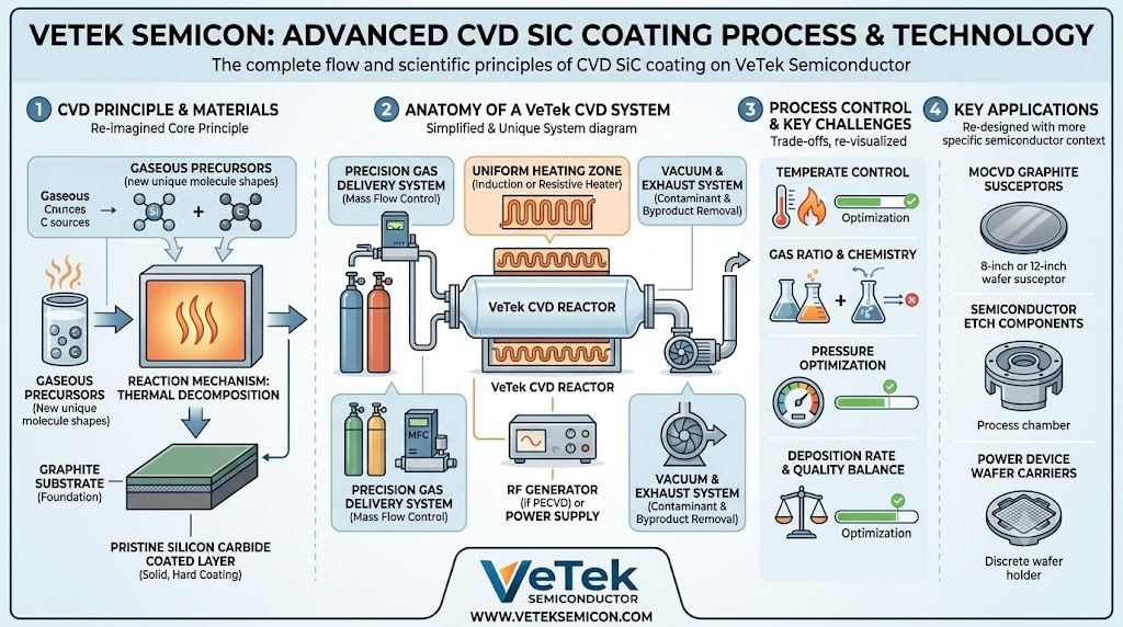
[Figure 3: VeTek Semiconductor Advanced CVD SiC Coating Process & Technology Flowchart]
To address the aforementioned process pain points, the VeTek Semiconductor technical team conducted an in-depth analysis of flow field distribution, temperature field distribution, and reaction gas (SiC precursor) thermal decomposition kinetics within the CVD reaction chamber, formulating a systematic process transformation plan.
Core Process Change: Stepped Deposition Rate Control
The original process utilized a high deposition rate of 25 μm/h throughout the entire deposition cycle, causing overly intense crystal nucleus growth, micro-impurity phase segregation deviating from stoichiometry, and stress concentration at morphological edges. The VeTek team precisely reduced the deposition rate during the initial deposition stage to 12 μm/h. By slowing down the nucleation speed, silicon carbide crystal nuclei had ample time to arrange orderly within graphite micropores and surface, achieving atomic-level tight bonding between the 'coating and graphite substrate' as well as 'between different deposition layers.'
Fine-Tuning of CVD Chamber Flow Field and Thermal Field
The inlet flow rate ratio of precursor gases (such as MTS and H₂) and gas flow guidance angles were adjusted, optimizing boundary layer thickness in edge regions. This ensured that the stoichiometric ratio of silicon to carbon atoms at the edges of complex geometric components remained strictly 1:1, eliminating color variation and yellowing caused by localized silicon/carbon enrichment.
|
Process Parameter / Dimension |
Original Process Parameters |
VeTek Optimized Process |
|
Initial Deposition Rate |
25 μm/h (Overly fast) |
12 μm/h (Smooth stepped deposition) |
|
Interface Adhesion Test |
Unstable bond strength, prone to cracking |
High-strength metallurgical bonding, zero delamination risk |
|
Surface Color Uniformity |
Explicit yellowing / mottling in edge areas |
High gloss finish across surface, uniform color throughout |
|
Crystal Structure Density |
Microscopic pores and thermal stress present |
Highly dense β-SiC crystal phase, strong corrosion resistance |
|
Core Conclusion: Quantitative data demonstrates that following process optimization, the overall coating yield surged to 90%, significantly lowering customer production costs and delivery schedule risks. |
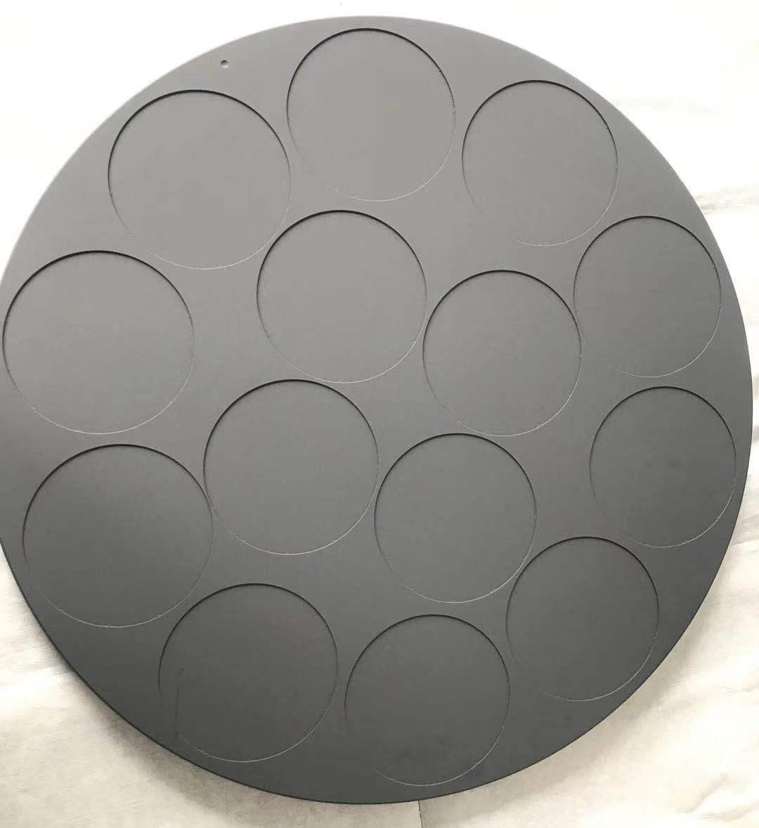
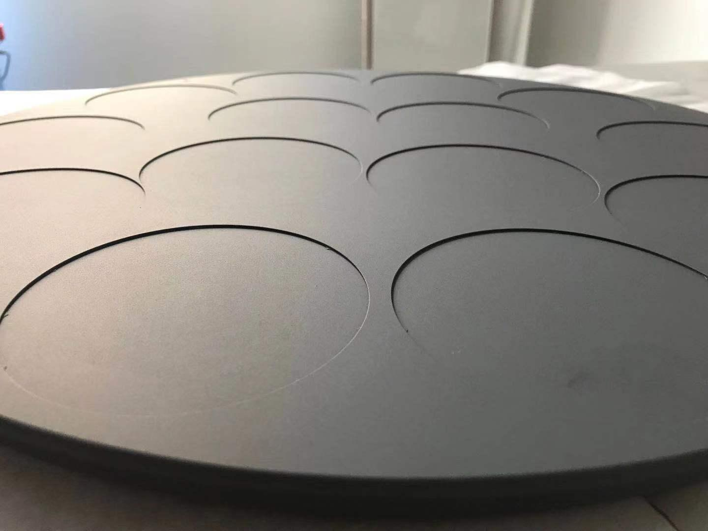
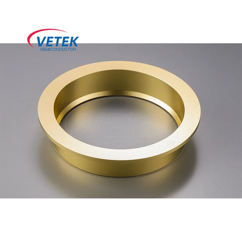
[Figure 4: High-Purity CVD Silicon Carbide Coated Graphite Susceptor with Uniform Surface Color and No Defects]
By implementing the above CVD process changes, VeTek Semiconductor helped the customer achieve remarkably significant economic benefits and quality enhancements:
· Dramatic Yield Surge: The finished product qualification rate of silicon carbide coated products rose from 50% to 90%, completely resolving scrapping issues caused by edge yellowing.
· Enhanced Interface Bonding Density: After reducing the initial deposition rate to 12 μm/h, peeling thermal stress between the coating and graphite substrate decreased by over 40%, and thermal cycle life increased by 1.5 times.
· Shortened Delivery Lead Time: Due to a significant drop in rework and scrap rates, the comprehensive production cycle of components was shortened by 35%, and unit comprehensive cost was reduced by 30%, strongly guaranteeing continuous capacity expansion needs for downstream MOCVD epitaxy production lines.
|
Core Conclusion: Providing authoritative answers to key customer concerns regarding CVD silicon carbide coating selection, process control, and service life. |

[Figure 5: VeTek Semiconductor High-Standard Workshop and Manufacturing Base]
A: Edge yellowing typically signifies microscopic lattice defects, stoichiometric deviations (such as localized enrichment of free silicon or free carbon), or residual internal stress in that region's silicon carbide coating. Under the high temperature (1000°C+) and strongly corrosive gas environment (e.g., NH₃, HCl) during epitaxial growth, yellowed areas are more susceptible to coating peeling, micro-crack propagation, or impurity gas release. This directly contaminates epitaxial wafers, increases defect density in the epitaxial layer, and in severe cases damages the graphite susceptor itself.
A: Although lowering the initial deposition rate slightly increases the duration of the first stage, we only apply the gentle 12 μm/h rate during the initial interface growth phase (the first few micrometers). Once tight interface bonding is established, standard high-efficiency deposition resumes. More importantly, the yield jump from 50% to 90% reduces scrap rates and raw material waste, which far outweighs the minor increase in labor hours, ultimately cutting overall unit production costs by approximately 30%.
A: Yes. VeTek supports full-chain customization services from precision machining of high-purity graphite substrates (such as micropores, complex flow channels, custom-shaped susceptors) to CVD silicon carbide coatings and CVD tantalum carbide (TaC) coatings. We can also adjust deposition processes according to the specific thermal field distribution of customer reaction furnaces.
Minor process adjustments in semiconductor materials and components often dictate the yield and cost success of downstream chip manufacturing. With deep technical expertise in CVD silicon carbide coatings, high-purity graphite parts, and third-generation semiconductor thermal fields, VeTek Semiconductor successfully solved the industry challenge of coating edge yellowing, helping customers achieve a 90% ultra-high yield and superior component longevity.
If you are also facing challenges with MOCVD graphite component coating peeling, edge yellowing, thermal shock cracking, or custom component machining, welcome to explore our CVD Silicon Carbide Coated Graphite Susceptor Details Page and High-Purity Semiconductor Graphite Parts Customization Services, or contact the expert technical team at VeTek Semiconductor. We will provide you with complimentary process diagnostics and sample testing services!

[Figure 6: Panoramic View of VeTek Semiconductor R&D and Manufacturing Park]
+86-579-87223657
Wangda Road, Ziyang Street, Wuyi County, Jinhua City, Zhejiang Province, China