
QR Code
Products
Contact Us


Fax
+86-579-87223657

E-mail

Address
Wangda Road, Ziyang Street, Wuyi County, Jinhua City, Zhejiang Province, China
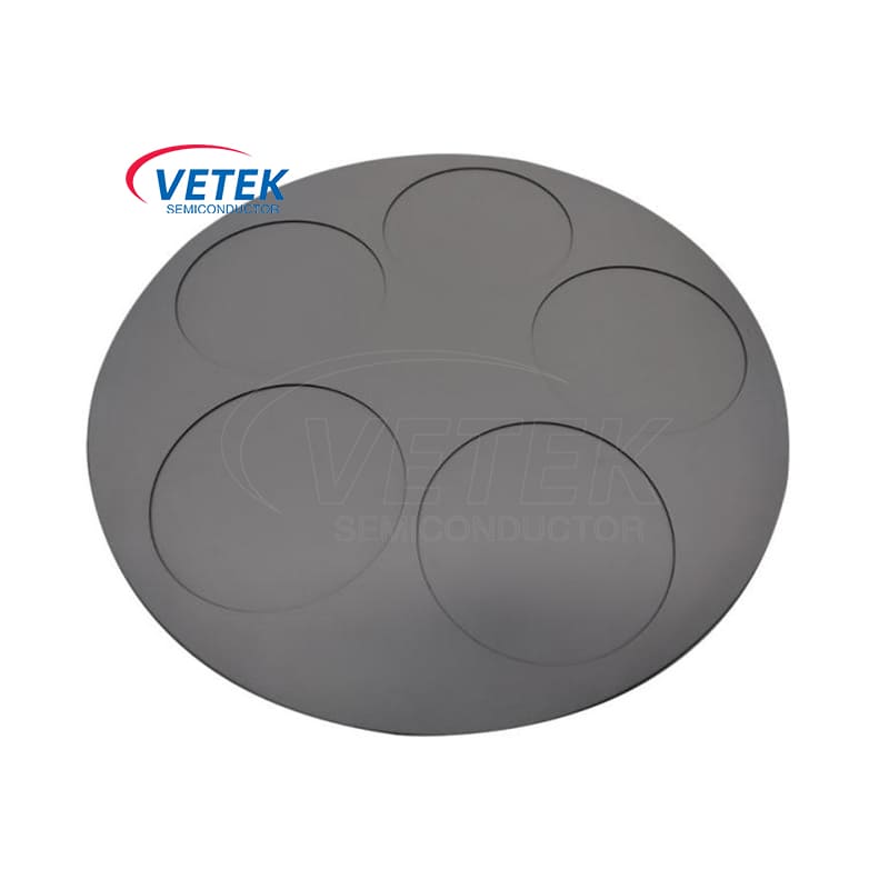
A CVD silicon carbide (SiC) coating is formed by exposing a heated graphite component to controlled precursor gases inside a chemical vapor deposition reactor. Reactive species reach the graphite surface, where SiC nucleates and grows into a dense polycrystalline layer. For semiconductor susceptors and wafer carriers, successful deposition depends on graphite purity, surface preparation, temperature, pressure, gas chemistry, mass transfer, geometry and thermal-expansion compatibility.
The goal is not simply to “cover” graphite, but to create a high-purity process surface with controlled thickness, roughness, stoichiometry and interface integrity.
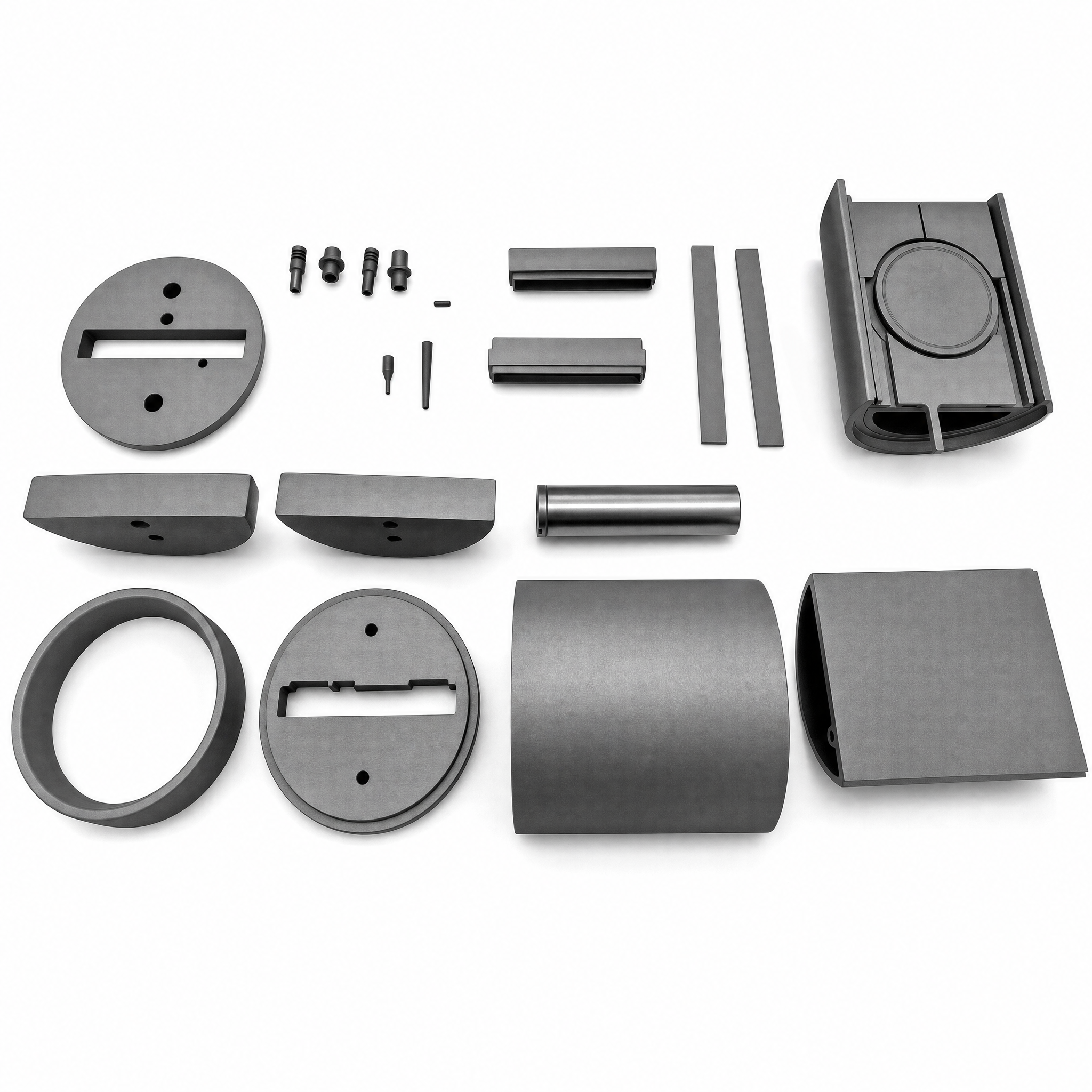
The process begins with substrate selection, machining and purification. High-purity isostatic graphite is commonly used because it combines machinability, thermal stability and a relatively uniform microstructure.
Key substrate factors include purity, density, porosity, grain structure and coefficient of thermal expansion (CTE). For susceptors and wafer carriers, machining accuracy is equally important because pocket depth, flatness, edge geometry and wall thickness can affect gas flow and final thermal behavior.
A simplified sequence is:
Graphite Selection → Precision Machining → Purification → Surface Preparation → CVD Deposition → Inspection
Before deposition, the surface must be clean and suitable for nucleation. Contamination, loose particles or local surface damage can disturb early SiC growth and later become weak regions, pinholes or non-uniform areas. Substrate preparation and coating deposition should therefore be treated as one integrated process.
A widely studied route uses methyltrichlorosilane (MTS, CH3SiCl3) as a single-source silicon-and-carbon precursor, with hydrogen and often argon in the gas system. At high temperature, MTS decomposes through gas-phase and surface reactions. Reactive species are transported through the boundary layer, adsorb on the hot graphite surface, react, and form solid SiC while volatile by-products are removed.
The deposition sequence can be simplified as:
Precursor Delivery → Gas Transport → Boundary-Layer Diffusion → Surface Adsorption → Nucleation → Grain Growth
Commercial CVD SiC deposition on graphite is commonly performed above about 1,200°C; SGL Carbon reports a typical range of 1,200–1,300°C for its process.
A 2026 Scientific Reports study using an MTS-H2 system examined 1,100–1,350°C and identified a transition near 1,180°C between stronger surface-reaction control and a regime where transport and diffusion become increasingly important.
At lower temperature, surface-reaction kinetics can limit deposition. As temperature rises, precursor decomposition accelerates. Once surface reactions are sufficiently fast, transport of reactive species through the gas boundary layer becomes more important.
For complex susceptors, coating uniformity is therefore also a fluid-dynamics problem.
CVD SiC quality is determined by several coupled variables, not by one “best” temperature.
|
Process Variable |
Main Influence |
|
Temperature |
Reaction rate, grain growth, morphology |
|
Pressure |
Mass transfer, roughness, porosity |
|
H2 / precursor ratio |
Si/C balance and phase purity |
|
Gas flow |
Boundary-layer behavior and uniformity |
|
Deposition time |
Coating thickness |
|
Component geometry |
Local flow and thickness distribution |
|
Surface condition |
Nucleation and interface quality |
Temperature strongly affects morphology. In the 2026 study, deposition near 1,200°C produced dense, well-defined β-SiC grains under the tested conditions, while excessive temperature promoted coarser structures.
Gas composition is equally important. In an MTS-H2 system, the hydrogen-to-MTS ratio changes carbon- and silicon-containing reaction pathways. The cited study obtained near-stoichiometric Si/C at an H2/MTS molar ratio around 10 under its conditions; this should be treated as a research example, not a universal industrial recipe.
Pressure and gas velocity influence how reactive species reach complex features. Sharp corners, deep pockets, grooves and shielded surfaces can develop different local boundary-layer conditions, so a coating uniform on a flat coupon may become non-uniform on a multi-pocket susceptor.
This is why CFD and reactor-flow optimization are useful for complex semiconductor parts.
The SiC/graphite interface is a major determinant of coating lifetime.
SiC is deposited at high temperature, and the component later experiences repeated heating and cooling during epitaxy or MOCVD. Because graphite and SiC do not expand identically, thermal strain develops during cooling and cycling.
A simplified failure pathway is:
CTE Mismatch + Residual Stress → Microcrack → Delamination → Particles / Exposed Graphite
Good coating design therefore requires a graphite grade with suitable thermal-expansion behavior, controlled surface condition and a deposition process that avoids excessive stress.
A 2026 Ceramics International study examining CVD SiC on graphite also showed that deposition temperature influences coating microstructure and interfacial adhesion.
Thickness matters as well. A thicker layer may increase the protective barrier, but it can also change component dimensions and increase accumulated stress. For semiconductor parts, coating thickness must therefore be considered together with geometry, flatness, surface finish and expected thermal cycles.
Coating defects are best understood by linking the visible symptom to its growth mechanism.
|
Defect / Symptom |
Possible Cause |
|
Pinholes |
Poor nucleation, particles, local growth gaps |
|
Rough surface |
Pressure or supersaturation conditions |
|
Non-uniform thickness |
Gas-flow or geometry-related mass transfer |
|
Cracking |
Residual stress, thermal cycling, CTE mismatch |
|
Delamination |
Weak interface or stress concentration |
|
Porosity |
Inappropriate growth conditions |
|
Edge peeling |
Geometry-driven stress or uneven deposition
|
Steps, corners, blind areas and wafer pockets can disturb gas flow. If reactive species are depleted before reaching a shielded region, local deposition rate can fall. Conversely, locally high supersaturation may promote rough or defect-prone growth.
The objective is not the highest deposition rate. Semiconductor coating requires a balance among density, purity, stoichiometry, surface roughness, thickness uniformity and interface integrity.
This is particularly important for multi-pocket MOCVD carriers and epitaxy susceptors, where different local flow conditions may exist across the same component.
After deposition, the coating should be evaluated as part of the finished component rather than as an isolated material.
Depending on the application, qualification may include:
l Dimensional inspection and flatness;
l Coating thickness and thickness uniformity;
l Surface roughness;
l Microscopy for cracks, pinholes or abnormal grains;
l Phase or microstructure analysis;
l Purity verification;
l Traceability and inspection documentation.
For epitaxy and MOCVD, the coating must also survive the real process environment. A coating that looks acceptable immediately after deposition may still degrade under repeated thermal cycles, aggressive cleaning chemistry or localized reactor conditions.
The engineering chain can therefore be summarized as:
CVD Recipe → Coating Structure → Interface Quality → Component Geometry → Thermal / Chemical Stability → Wafer Process Performance
This relationship explains why CVD SiC coating should be specified using performance-relevant parameters rather than nominal coating thickness alone.
For a susceptor or wafer carrier, coating quality ultimately has to work together with graphite quality, precision machining and component geometry to support stable thermal behavior, low contamination and repeatable semiconductor processing.
1. What precursor is commonly used for CVD SiC coating on graphite?
Methyltrichlorosilane (MTS) is widely studied because it contains both silicon and carbon. Actual production chemistry and deposition recipes vary by manufacturer, reactor and application.
2. What temperature is used to deposit CVD SiC on graphite?
Commercial and research processes commonly operate above 1,200°C, but the optimum temperature depends on reactor design, pressure, precursor chemistry, graphite grade and required coating structure.
3. What controls SiC coating thickness uniformity?
Gas flow, pressure, component geometry, deposition time, temperature distribution and precursor transport all matter. Deep pockets, corners and shielded surfaces are particularly sensitive to local mass-transfer conditions.
4. Why can CVD SiC coating crack or delaminate?
Typical contributors include residual stress, graphite/SiC CTE mismatch, inadequate interface preparation, coating microstructural defects and repeated thermal cycling.
5. What information should be supplied for a CVD SiC coating RFQ?
Provide the 2D drawing or 3D model, component function, reactor model, process conditions, graphite requirement, coating thickness, surface roughness, dimensional tolerances, inspection requirements and required quantity.
1. SGL Carbon. SIGRAFINE® SiC Coating — CVD SiC deposition on isostatic graphite, coating temperature and thermal-expansion matching.
2. Huo, Y. et al. Study of the process-structure-property correlation in CVD-SiC coatings on graphite substrates. Scientific Reports, Vol. 16, Article 4150, 2026.
3. Ma, Q. et al. Interfacial adhesion of CVD-SiC coatings on graphite substrates: Role of temperature in microstructure and mechanical properties. Ceramics International, Vol. 52, 2026.
4. Zhu, D., Hing, P., Brown, P., Sahai, Y. Characterization of silicon carbide coatings grown on graphite by chemical vapor deposition. Journal of Materials Processing Technology, Vol. 48, 1995.


+86-579-87223657


Wangda Road, Ziyang Street, Wuyi County, Jinhua City, Zhejiang Province, China
Copyright © 2024 WuYi TianYao New Material Tech.Co.,Ltd. All Rights Reserved.
Links | Sitemap | RSS | XML | Privacy Policy |