We are glad to share with you about the results of our work, company news,and give you timely developments and personnel appointment and removal conditions.
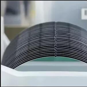
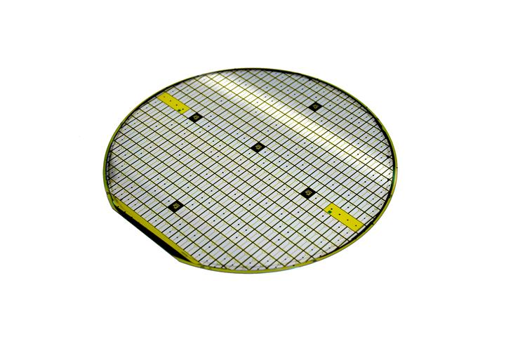
Silicon wafers are the foundation of integrated circuits and semiconductor devices. They have an interesting feature - flat edges or tiny grooves on the sides .It is not a defect, but a deliberately designed functional marker.In fact, this notch serves as a directional reference and identity marker throughout the entire manufacturing process.
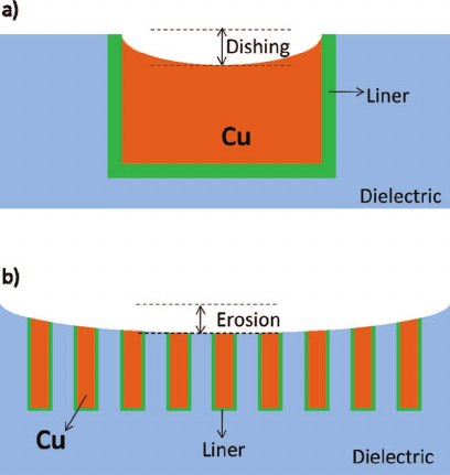
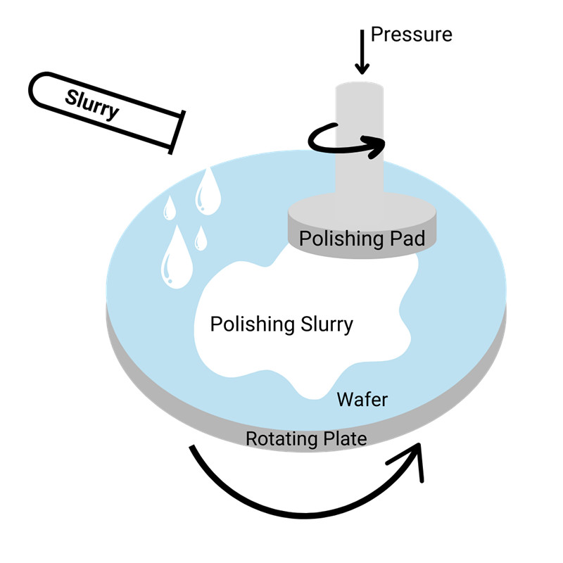
Chemical mechanical polishing (CMP) removes excess material and surface defects through the combined action of chemical reactions and mechanical abrasion. It is a key process for achieving global planarization of the wafer surface and is indispensable for multilayer copper interconnects and low-k dielectric structures. In practical manufacturing
Silicon wafer CMP (Chemical Mechanical Planarization) polishing slurry is a critical component in the semiconductor manufacturing process. It plays a pivotal role in ensuring that silicon wafers—used to create integrated circuits (ICs) and microchips—are polished to the exact level of smoothness required for the next stages of production
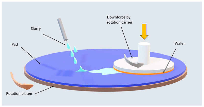
In semiconductor manufacturing, Chemical Mechanical Planarization (CMP) plays a vital role. The CMP process combines chemical and mechanical actions to smooth the surface of silicon wafers, providing a uniform foundation for subsequent steps such as thin-film deposition and etching. CMP polishing slurry, as the core component of this process, significantly impacts polishing efficiency, surface quality, and the final performance of the product
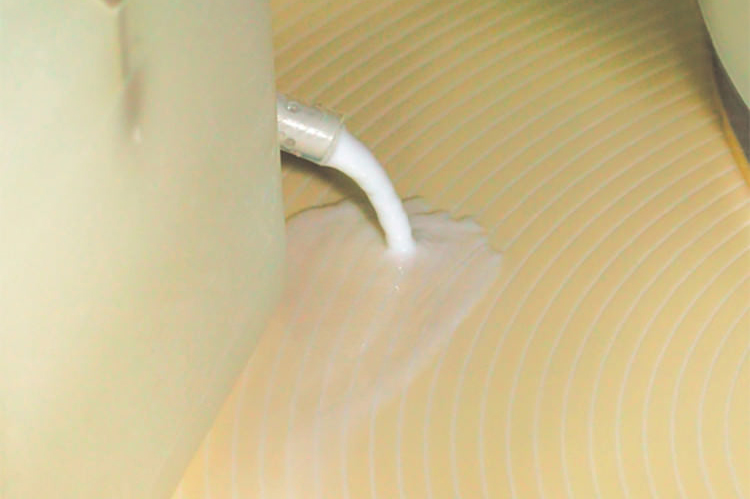
Wafer CMP polishing slurry is a specially formulated liquid material used in the CMP process of semiconductor manufacturing. It consists of water, chemical etchants, abrasives, and surfactants, enabling both chemical etching and mechanical polishing.
Silicon carbide abrasives are typically produced using quartz and petroleum coke as primary raw materials. In the preparatory stage, these materials undergo mechanical processing to achieve the desired particle size before being chemically proportioned into furnace charge.
Over the past few years, the center stage of packaging technology has gradually been ceded to a seemingly "old technology" - CMP (Chemical Mechanical Polishing). When Hybrid Bonding becomes the leading role of the new generation of advanced packaging, CMP is gradually moving from behind the scenes to the spotlight.
In the ever-evolving world of home and kitchen appliances, one product has recently gained significant attention for its innovation and practical application—the Quartz Thermos Bucket
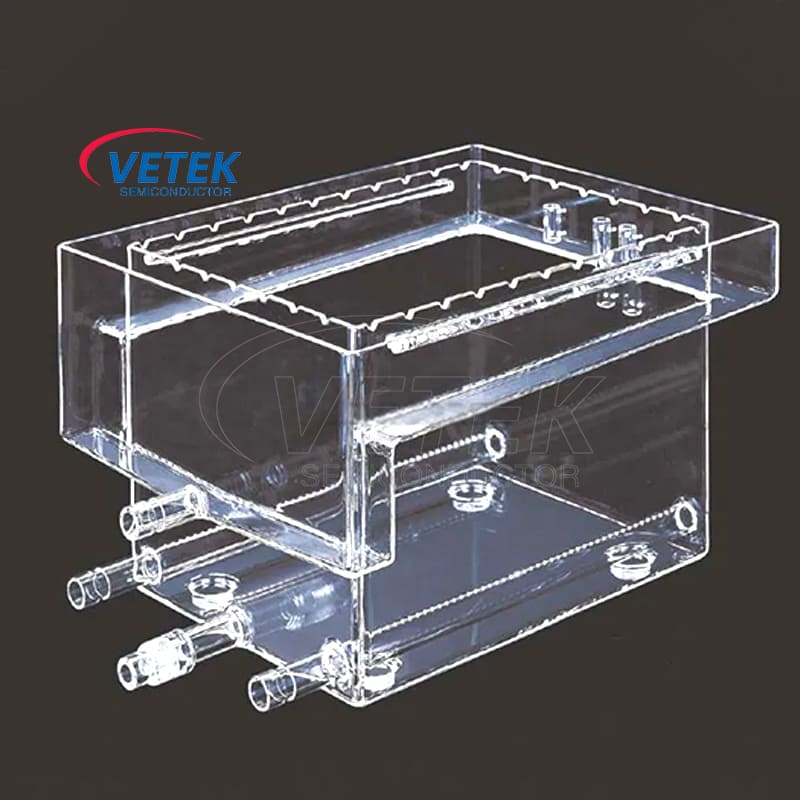
Quartz products are widely used in the semiconductor manufacturing process due to their high purity, high-temperature resistance, and strong chemical stability.
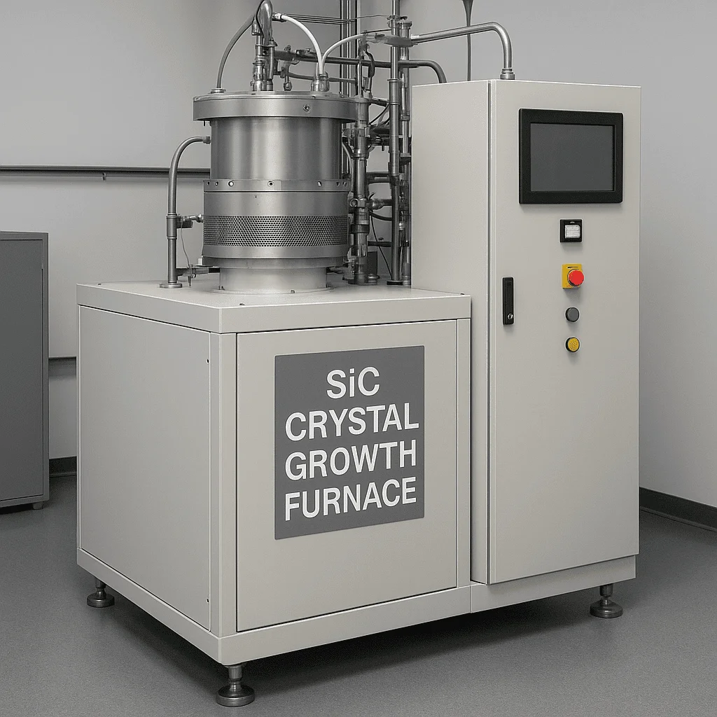
Silicon carbide (SiC) crystal growth furnaces play a vital role in producing high-performance Sic wafers for next-generation semiconductor devices. However, the process of growing high-quality SiC crystals presents significant challenges. From managing extreme thermal gradients to reducing crystal defects, ensuring uniform growth, and controlling production costs, each step requires advanced engineering solutions. This article will analyze the technical challenges of SIC crystal growth furnaces from multiple perspectives.
Smart cut is an advanced semiconductor manufacturing process based on ion implantation and wafer stripping, specifically designed for the production of ultra-thin and highly uniform 3C-SiC (cubic silicon carbide) wafers. It can transfer ultra-thin crystal materials from one substrate to another, thereby breaking the original physical limitations and changing the entire substrate industry.
In the preparation of high-quality and high-yield silicon carbide substrates, the core requires precise control of production temperature by good thermal field materials. Currently, the thermal field crucible kits mainly used are high-purity graphite structural components, whose functions are to heat molten carbon powder and silicon powder as well as to maintain heat.
When you see the third-generation semiconductors, you will surely wonder what the first and second generations were. The "generation" here is classified based on the materials used in semiconductor manufacturing.
The electrostatic chuck(ESC), also known as the electrostatic chuck (ESC, e-chuck), is a fixture that uses the principle of electrostatic adsorption to hold and fix the adsorbed material. It is suitable for vacuum and plasma environments.
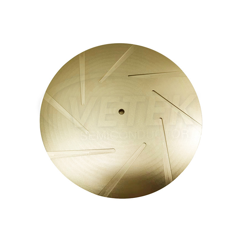
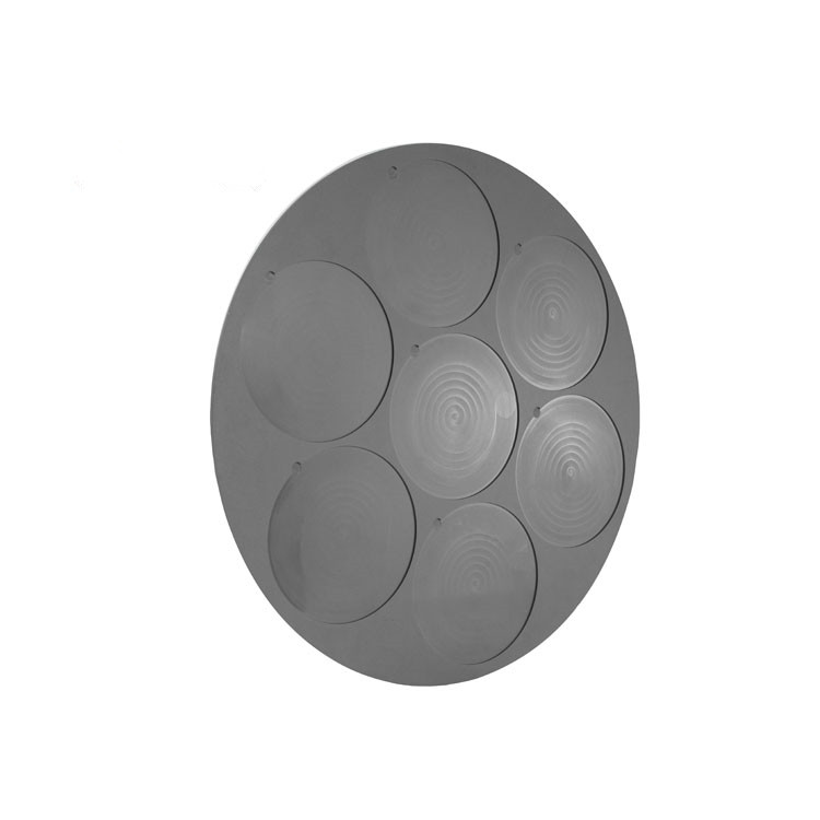
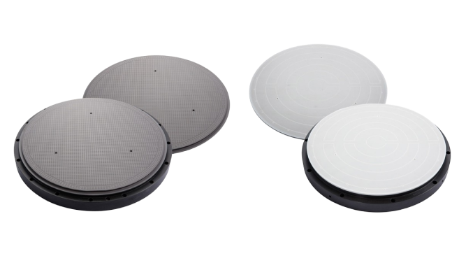
SiC wafer carriers, as key consumables in the third-generation semiconductor industry chain, their technical characteristics directly affect the yield of epitaxial growth and device manufacturing. With the surging demand for high-voltage and high-temperature devices in industries such as 5G base stations and new energy vehicles, the research and application of SiC wafer carriers are now facing significant development opportunities.
We use cookies to offer you a better browsing experience, analyze site traffic and personalize content. By using this site, you agree to our use of cookies. Privacy Policy