We are glad to share with you about the results of our work, company news,and give you timely developments and personnel appointment and removal conditions.
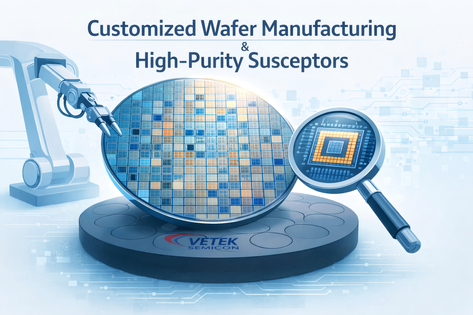
As semiconductor manufacturing continues to evolve toward advanced process nodes, higher integration, and complex architectures, the decisive factors for wafer yield are undergoing a subtle shift. For customized semiconductor wafer manufacturing, the breakthrough point for yield no longer lies solely in core processes like lithography or etching; high-purity susceptors are increasingly becoming the underlying variable affecting process stability and consistency.
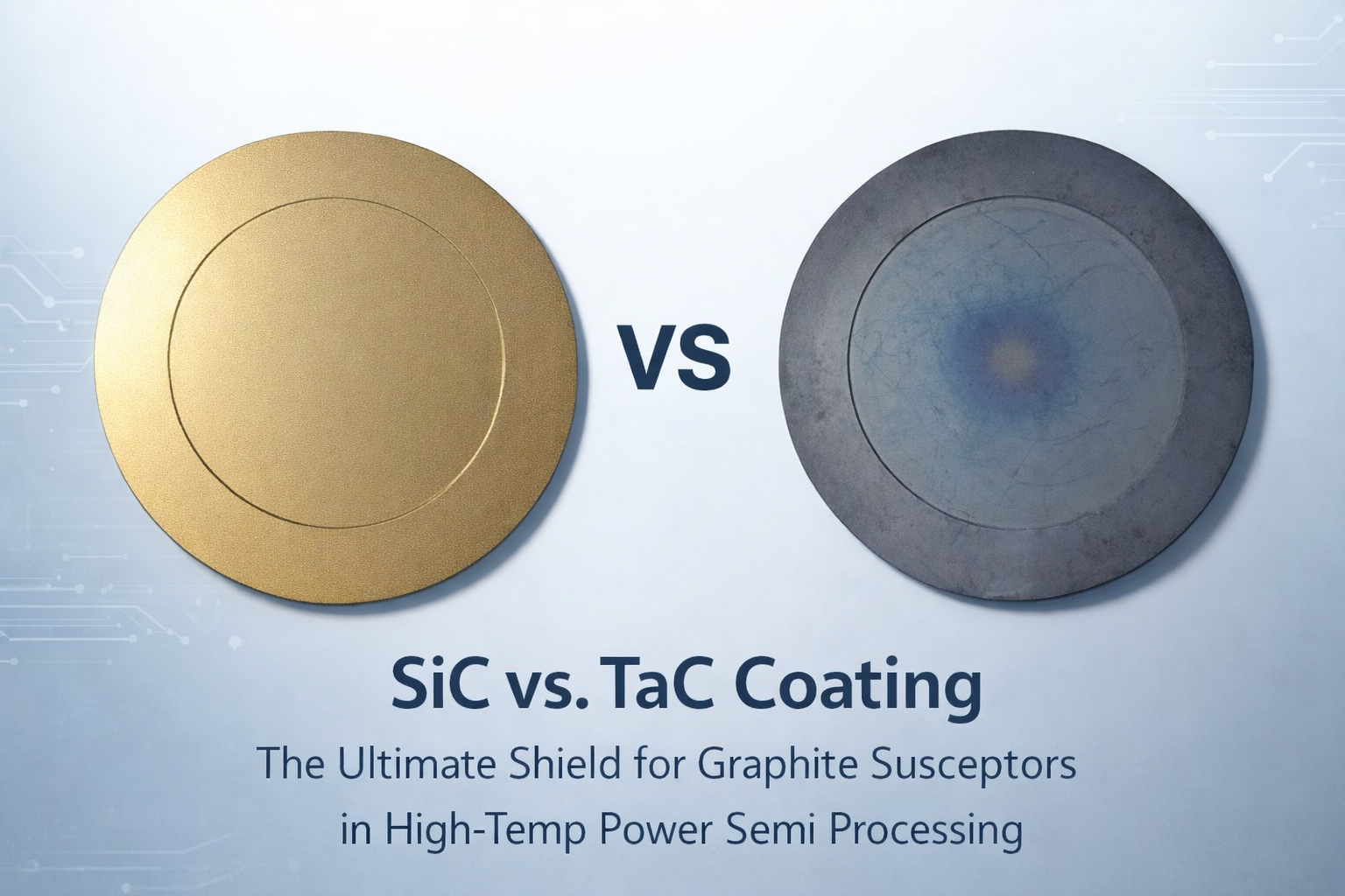
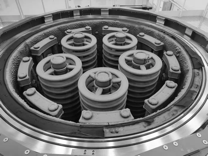
In the world of wide-bandgap (WBG) semiconductors, if the advanced manufacturing process is the "soul," the graphite susceptor is the "backbone," and its surface coating is the critical "skin."
In the high-stakes world of power electronics, Silicon Carbide (SiC) and Gallium Nitride (GaN) are spearheading a revolution—from Electric Vehicles (EVs) to renewable energy infrastructure. However, the legendary hardness and chemical inertness of these materials present a formidable manufacturing bottleneck.
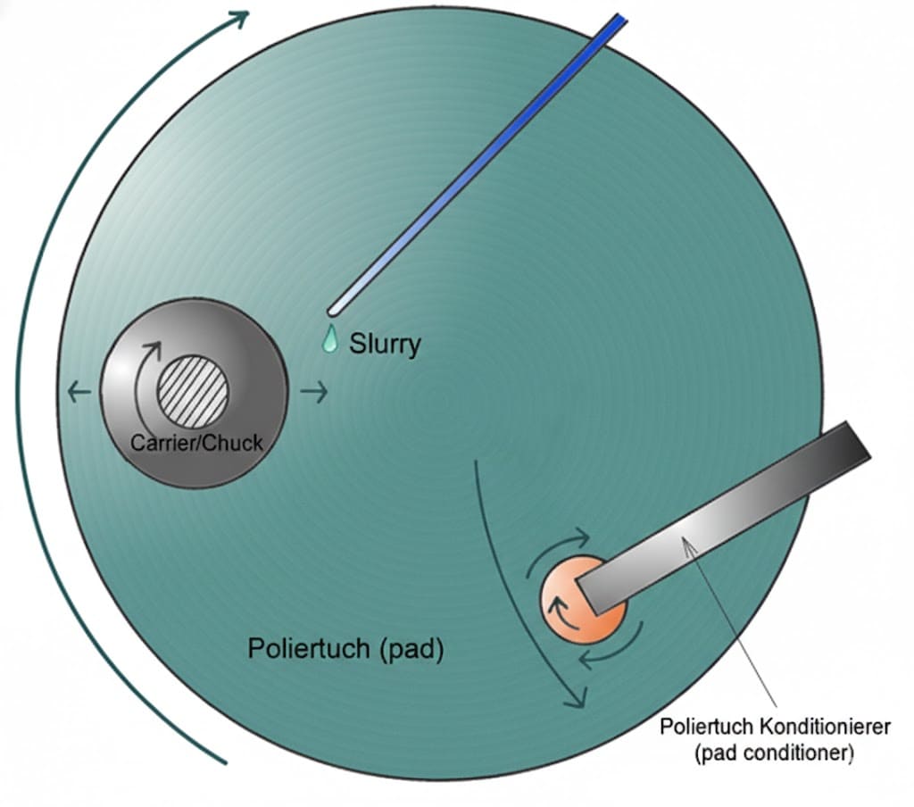
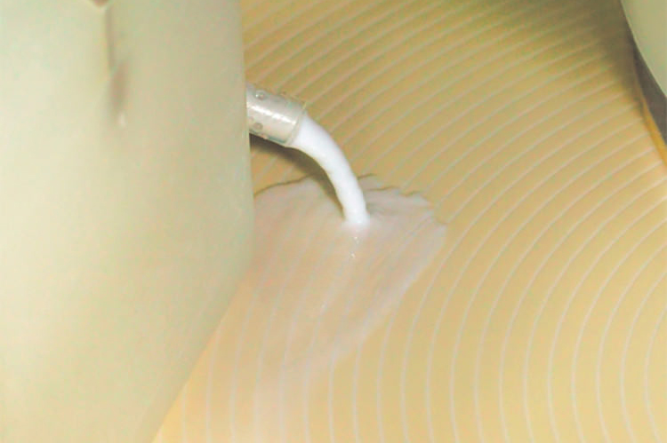
In semiconductor manufacturing, the Chemical Mechanical Planarization (CMP) process is the core stage for achieving wafer surface planarization, directly determining the success or failure of subsequent lithography steps. As the critical consumable in CMP, the performance of the Polishing Slurry is the ultimate factor in controlling Removal Rate (RR), minimizing defects, and enhancing overall yield.
In the high-stakes world of semiconductor manufacturing, where precision and extreme environments coexist, Silicon Carbide (SiC) focus rings are indispensable. Known for their exceptional thermal resistance, chemical stability, and mechanical strength, these components are critical to advanced plasma etching processes.
The secret behind their high performance lies in Solid CVD (Chemical Vapor Deposition) technology. Today, we take you behind the scenes to explore the rigorous manufacturing journey—from a raw graphite substrate to a high-precision "invisible hero" of the fab.
High-purity quartz materials play a vital role in the semiconductor industry. Their superior high-temperature resistance, corrosion resistance, thermal stability, and light transmission properties make them critical consumables. Quartz products are used for components in both high-temperature and low-temperature zones of wafer production, ensuring the stability and cleanliness of the manufacturing process.
We use cookies to offer you a better browsing experience, analyze site traffic and personalize content. By using this site, you agree to our use of cookies.
Privacy Policy