


QR Code

Products
Contact Us


Fax
+86-579-87223657

E-mail

Address
Wangda Road, Ziyang Street, Wuyi County, Jinhua City, Zhejiang Province, China


As a leading professional manufacturer in the field, VeTek Semiconductor is delighted to offer you top-notch PSS Etching Carrier Plates tailored specifically for the semiconductor industry.
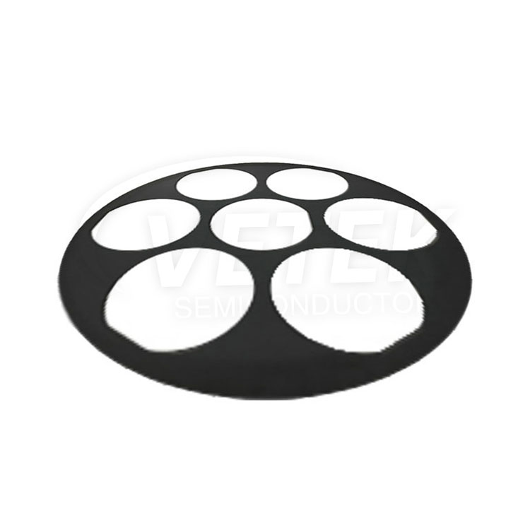
Our PSS Etching Carrier Plates for Semiconductors are highly specialized components that are indispensable in the Plasma Source Spectroscopy (PSS) etching procedures within the semiconductor manufacturing realm. These plates assume a pivotal role during the etching process. They provide stable support and ensure smooth transportation of semiconductor wafers, which is crucial for the precision and quality of the etching operation.
We warmly invite you to reach out to us for any inquiries. We're always ready to assist and provide more detailed information about our outstanding products.
● Precision Design: The carrier plate is engineered with precise dimensions and surface flatness to ensure uniform and consistent etching across the semiconductor wafers. It provides a stable and controlled platform for the wafers, allowing for accurate and reliable etching results.
● Plasma Resistance: The carrier plate exhibits excellent resistance to the plasma used in the etching process. It remains unaffected by the reactive gases and high-energy plasma, ensuring prolonged service life and consistent performance.
● Thermal Conductivity: The carrier plate features high thermal conductivity to efficiently dissipate heat generated during the etching process. This helps in maintaining optimal temperature control and prevents overheating of the semiconductor wafers.
● Compatibility: The PSS Etching Carrier Plate is designed to be compatible with various semiconductor wafer sizes commonly used in the industry, ensuring versatility and ease of use across different manufacturing processes.
| Basic physical properties of CVD SiC coating | |
| Property | Typical Value |
| Crystal Structure | FCC β phase polycrystalline, mainly (111) oriented |
| SiC coating Density | 3.21 g/cm³ |
| CVD SiC coating Hardness | 2500 Vickers hardness(500g load) |
| Grain Size | 2~10 μm |
| Chemical Purity | 99.99995% |
| Heat Capacity | 640 J·kg-1·K-1 |
| Sublimation Temperature | 2700 ℃ |
| Flexural Strength | 415 MPa RT 4-point |
| Young's Modulus | 430 Gpa 4pt bend, 1300℃ |
| Thermal Conductivity | 300W·m-1·K-1 |
| Thermal Expansion(CTE) | 4.5×10⁻⁶K-1 |


Address
Wangda Road, Ziyang Street, Wuyi County, Jinhua City, Zhejiang Province, China
Tel
+86-579-87223657
Wangda Road, Ziyang Street, Wuyi County, Jinhua City, Zhejiang Province, China