


QR Code

Products
Contact Us


Fax
+86-579-87223657

E-mail

Address
Wangda Road, Ziyang Street, Wuyi County, Jinhua City, Zhejiang Province, China


1.The defect density has decreased significantly
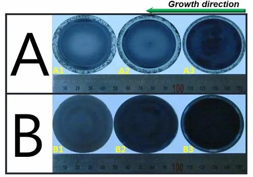
The TaC coating almost completely eliminates the carbon encapsulation phenomenon by isolating the direct contact between the graphite crucible and the SiC melt, significantly reducing the defect density of microtubes. Experimental data show that the density of microtube defects caused by carbon coating in the crystals grown in TaC coated crucibles is reduced by more than 90% compared with traditional graphite crucibles. The crystal surface is uniformly convex, and there is no polycrystalline structure at the edge, while ordinary graphite crucibles often have edge polycrystallization and crystal depression and other defects.
2. Impurity inhibition and purity improvement
TaC material has excellent chemical inertness to Si, C and N vapors and can effectively prevent impurities such as nitrogen in graphite from diffusing into the crystal. GDMS and Hall tests show that the nitrogen concentration in the crystal has decreased by more than 50%, and the resistivity has increased to 2-3 times that of the traditional method. Although a trace amount of Ta element was incorporated (atomic proportion < 0.1%), the overall total impurity content was reduced by more than 70%, significantly improving the electrical properties of the crystal.
3. Crystal morphology and growth uniformity
The TaC coating regulates the temperature gradient at the crystal growth interface, enabling the crystal ingot to grow on a convex curved surface and homogenizing the edge growth rate, thus avoiding the polycrystallization phenomenon caused by edge overcooling in traditional graphite crucibles. The actual measurement shows that the diameter deviation of the crystal ingot grown in the TaC coated crucible is ≤2%, and the crystal surface flatness (RMS) is improved by 40%.
|
Characteristic |
TaC Coating Mechanism |
Impact on Crystal Growth |
|
Thermal Conductivity & Temperature Distribution |
Thermal conductivity (20-22 W/m·K) is significantly lower than graphite (>100 W/m·K), reducing radial heat dissipation and decreasing radial temperature gradient in the growth zone by 30% |
Improved temperature field uniformity, reducing lattice distortion caused by thermal stress and decreasing defect generation probability |
|
Radiative Heat Loss |
Surface emissivity (0.3-0.4) is lower than graphite (0.8-0.9), reducing radiative heat loss and allowing heat to return to the furnace body via convection |
Enhanced thermal stability around the crystal, leading to more uniform C/Si vapor concentration distribution and reducing defects caused by compositional supersaturation |
|
Chemical Barrier Effect |
Prevents reaction between graphite and Si vapor at high temperatures (Si + C → SiC), avoiding additional carbon source release |
Maintains ideal C/Si ratio (1.0-1.2) in the growth zone, suppressing inclusion defects caused by carbon supersaturation |
|
Material Type |
Temperature Resistance |
Chemical Inertness |
Mechanical Strength |
Crystal Defect Density |
Typical Application Scenarios |
|
TaC Coated Graphite |
≥2600°C |
No reaction with Si/C vapor |
Mohs Hardness 9-10, strong thermal shock resistance |
<1 cm⁻² (micropipes) |
High-purity 4H/6H-SiC single crystal growth |
|
Bare Graphite |
≤2200°C |
Corroded by Si vapor releasing C |
Low strength, prone to cracking |
10-50 cm⁻² |
Cost-effective SiC substrates for power devices |
|
SiC Coated Graphite |
≤1600°C |
Reacts with Si forming SiC₂ at high temperatures |
High hardness but brittle |
5-10 cm⁻² |
Packaging materials for mid-temperature semiconductors |
|
BN Crucible |
<2000K |
Releases N/B impurities |
Poor corrosion resistance |
8-15 cm⁻² |
Epitaxial substrates for compound semiconductors |
The TaC coating has achieved a comprehensive improvement in the quality of SiC crystals through a triple mechanism of chemical barrier, thermal field optimization and interface regulat
+86-579-87223657
Wangda Road, Ziyang Street, Wuyi County, Jinhua City, Zhejiang Province, China