QR Code

Products
Contact Us


Fax
+86-579-87223657

Email

Address
Wangda Road, Ziyang Street, Wuyi County, Jinhua City, Zhejiang Province, China


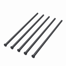
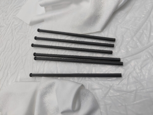
Figure 1: AMAT 0200-03201 Hollow Lift Pin physical product (for 300 mm silicon epitaxy systems)
In semiconductor wafer transfer processes, the hollow lift pin (Wafer Lift Pin) undertakes the critical tasks of supporting and transferring wafers. In high-temperature process environments such as MOCVD and epitaxial growth, lift pins must simultaneously meet multiple requirements including high purity, corrosion resistance, thermal shock resistance, and low particle contamination.
Currently, the mainstream lift pins on the market adopt a graphite substrate + CVD SiC coating solution. However, the coating technology of the vast majority of suppliers can only cover the outer surface—for hollow structures, the inner wall is truly the “technical no-man's land”.
1. Uncontrolled Deposition Uniformity
Hollow structures have a large aspect ratio. CVD reactant gases struggle to diffuse uniformly deep into the internal bore, causing the inner-wall coating thickness to decrease in a gradient from the port to the deep interior, with local areas even showing bare exposed regions.
2. Insufficient Interfacial Bonding Strength
The curved inner-wall surface limits the optimization space of deposition process parameters. The bonding strength between the coating and the graphite substrate is difficult to reach the same level as the outer surface, and micro-cracks or even peeling can easily occur during thermal cycling.
3. Uncontrolled Internal Bore Cleanliness
If the porous structure of the graphite substrate is not completely sealed by the coating, carbon particles and metallic impurities will be released at high temperatures. Once impurities detach, they directly cause color difference and particle defects on the wafer surface, severely lowering production yield.
Leveraging its deep technical expertise accumulated in the CVD coating field, VETEK has successfully overcome the challenges of uniform deposition and interfacial bonding of CVD SiC coating on the inner wall of hollow structures—from gas flow field simulation optimization to precise deposition temperature field control, establishing a complete inner-wall coating process solution that ensures consistent coating thickness from the port to the deep interior of the bore, firm bonding, and internal bore cleanliness meeting standards.
This article will provide an in-depth analysis of: the technical difficulties of hollow lift pin inner-wall coating, how inner-wall coating uniformity affects wafer yield, and the key control nodes from process design to quality control and delivery.
|
Core Conclusion: An AMAT hollow lift pin is a precision wafer handling component whose internal cavity reduces thermal mass while maintaining the mechanical strength required for reliable wafer lifting and positioning. |
An AMAT hollow lift pin is a precision wafer handling component used inside semiconductor process equipment. Its primary function is to lift and position wafers during loading, unloading, and process sequences.
Unlike conventional solid lift pins, the hollow design incorporates an internal cavity. This structure reduces overall material volume and thermal mass while maintaining the required mechanical geometry. However, for semiconductor applications, manufacturing hollow lift pins is far more demanding than machining conventional solid components. Dimensional accuracy of both inner and outer surfaces must be strictly controlled, and concentricity between the inner and outer geometries is particularly critical. Therefore, both material selection and coating processes are essential to the final performance of the lift pin.
For AMAT epitaxy systems, VETEK Semiconductor provides customized AMAT hollow lift pin solutions based on high-purity graphite substrates and dense CVD silicon carbide (SiC) coatings. The hollow structure helps reduce unnecessary material mass while maintaining the mechanical structure required for wafer lifting; the CVD silicon carbide coating provides high purity, chemical resistance, and high-temperature stability. VETEK's AMAT 0200-03201 lift pin is specifically designed for 300 mm silicon epitaxy applications and can be manufactured according to customer drawings, dimensions, and process requirements.
|
Core Conclusion: VETEK adopts a high-purity graphite substrate + dense CVD silicon carbide coating structure, balancing excellent machinability with semiconductor-grade surface purity and protection performance. |
VETEK currently focuses on the high-purity graphite + CVD silicon carbide coating structure for AMAT hollow lift pins. The basic construction process is:
High-purity graphite substrate → Precision CNC machining → CVD silicon carbide coating → Precision inspection
The graphite substrate provides the structural foundation and is suitable for precision machining of thin-wall and hollow geometries. VETEK typically uses imported semiconductor-grade graphite materials, including materials from SGL Carbon and Toyo Tanso, depending on customer requirements. A dense CVD silicon carbide coating is then deposited on the graphite surface to form a protective semiconductor-grade working surface.
For hollow lift pins, the substrate material must strike a balance among machinability, thermal performance, mechanical stability, and coating process compatibility. High-purity graphite is particularly suitable because it offers the following characteristics:
• Good high-temperature stability
• Low thermal expansion
• Good thermal conductivity
• Relatively low density
• Excellent machinability for complex geometries
• Compatibility with the CVD silicon carbide coating process
The use of graphite also makes it possible to manufacture complex hollow and thin-wall structures with high precision. VETEK possesses precision CNC machining capabilities for semiconductor graphite and silicon carbide components, with machining processes optimized for dimensional control and surface quality.
|
Core Conclusion: A dense CVD silicon carbide coating of approximately 100±20 μm thickness and 6N purity protects the graphite substrate and provides a stable high-purity working surface for the semiconductor environment. |
The CVD silicon carbide coating is one of the most important features of VETEK AMAT hollow lift pins. This coating forms a dense silicon carbide surface on the graphite substrate, helping to protect the underlying graphite from the process environment.
The standard CVD silicon carbide coating thickness for such VETEK components is approximately 100±20 μm. The coating purity is approximately 6N / 99.99995%.
VETEK's broader CVD silicon carbide technical capabilities include high-purity coatings, controlled coating thickness, and batch-to-batch thickness uniformity. Technical data indicate that CVD silicon carbide coating purity is at the 6N–7N level. For specific AMAT lift pin projects, coating specifications can be adjusted according to customer drawings and process requirements.
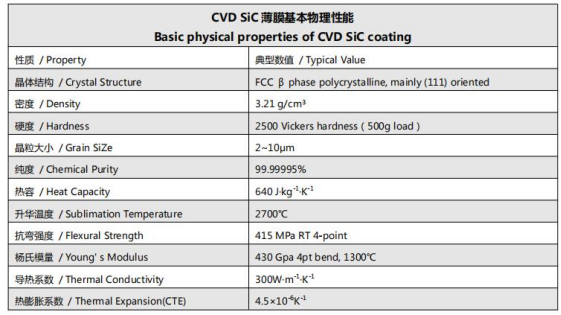
Figure 2: Basic physical properties of CVD SiC coating
One of the most technically challenging aspects of AMAT hollow lift pins is not merely coating the outer surface, but achieving a stable and uniform coating on the inner wall of the hollow structure.
The inner surface is difficult to access during the CVD coating process. Compared with the outer surface, the internal geometry introduces additional challenges in gas flow, deposition uniformity, coating thickness control, and process consistency. Therefore, inner-wall coating quality can become an important differentiating factor among suppliers.
VETEK has experience in CVD silicon carbide coating of hollow structures and places special emphasis on the inner surface. A well-controlled inner-wall coating helps maintain a protective silicon carbide layer throughout the hollow structure, rather than leaving the internal graphite exposed to the process environment. This is particularly important when the lift pin operates in high-temperature and chemically aggressive semiconductor process chambers.
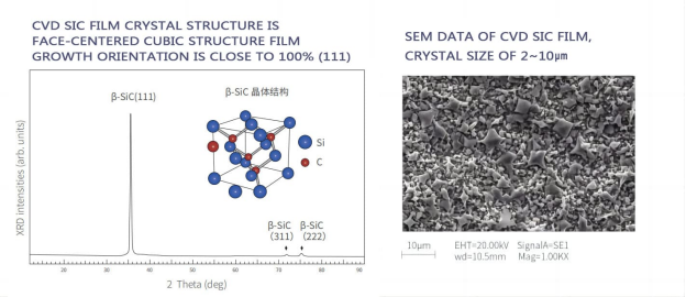
Figure 3: Microscopic crystal structure of CVD silicon carbide coating
|
Core Conclusion: High-purity material system, controlled coating thickness, excellent inner-wall coverage, high-temperature stability, chemical and corrosion resistance, precision machining, and comprehensive customization capabilities. |
High-purity material system: The combination of high-purity graphite and high-purity CVD silicon carbide is designed for semiconductor environments where contamination control is critical. Depending on the selected specification, the CVD silicon carbide coating purity is 6N.
Standard 100±20 μm silicon carbide coating: VETEK's standard coating thickness is approximately 100±20 μm, providing a practical coating thickness for semiconductor process components, while customization is available according to customer requirements.
Excellent inner-wall coating capability: For hollow components, inner-wall coating is one of the more difficult parts of the manufacturing process. VETEK has developed coating processes capable of achieving high-quality coverage on the inner wall of hollow lift pins, from gas flow field simulation to temperature field control, ensuring consistent coating thickness, firm bonding.
High-temperature stability: Both the graphite substrate and the CVD silicon carbide coating are suitable for high-temperature semiconductor process environments. The CVD silicon carbide layer provides additional protection against chemical attack and surface degradation. VETEK’s CVD silicon carbide film data list high thermal conductivity, low thermal expansion, and a sublimation temperature of approximately 2700 °C, indicating that the material is suitable for demanding high-temperature applications.
Chemical and corrosion resistance: The dense CVD silicon carbide surface offers better corrosion resistance than bare graphite and can withstand aggressive process gases and chemical cleaning environments. This helps reduce substrate degradation and maintains a more stable component surface over repeated process cycles.
Precision machining and customization: Hollow lift pins require precise control of outer diameter, inner diameter, wall thickness, length, and concentricity. VETEK combines CNC precision machining with CVD coating processes to manufacture complex semiconductor components according to customer drawings. Lift pins can be manufactured according to:
• Customer drawings
• Sample components
• Dimensional specifications
• Required coating thickness
• Required graphite grade
• Specific process requirements
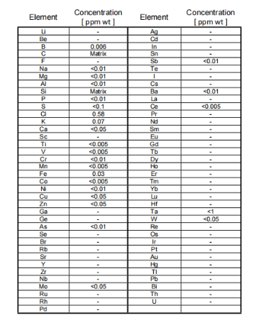
Figure 4: CVD silicon carbide coating GDMS purity test report
|
Core Conclusion: Primarily used for wafer handling in 300 mm wafer silicon epitaxy systems, and more broadly applicable to other high-temperature semiconductor process equipment. |
Silicon epitaxy: Lift pins are used for wafer lifting, positioning, and transfer within epitaxy equipment. VETEK's existing AMAT 0200-03201 product is specifically positioned for 300 mm silicon epitaxy applications.
Wafer handling systems: Lift pins can serve as precision wafer handling components for applications requiring high-temperature stability, dimensional accuracy, and contamination control. Wafer lift pins with a hollow tubular body can effectively minimize local heat loss, thereby reducing the pin marks commonly seen on the wafer backside in high-temperature processes (such as epitaxial growth or annealing). Forming a hollow cavity inside the lift pin body reduces thermal mass and improves wafer temperature uniformity.
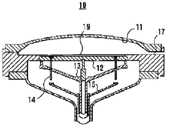
Figure 5: Schematic of the principle by which hollow lift pins reduce thermal mass and improve wafer temperature uniformity
Semiconductor process equipment: Based on customer drawings and samples, similar graphite + CVD silicon carbide components can be developed for other semiconductor equipment platforms. VETEK's semiconductor product portfolio covers silicon epitaxy, silicon carbide epitaxy, MOCVD, RTP/RTA, etching, and other semiconductor processes.
|
Core Conclusion: An integrated process flow from high-purity graphite selection and precision CNC machining, through CVD silicon carbide coating (including inner wall), to final inspection. |
The production of AMAT hollow lift pins involves multiple critical steps, each of which directly affects the reliability of the final product and wafer yield:
1. Graphite material selection — Select the appropriate high-purity graphite grade (SGL Carbon or Toyo Tanso, etc.) according to the customer’s dimensional, thermal performance, and purity requirements.
2. Precision CNC machining — Machine the graphite blank into the required hollow geometry. Special attention is paid to inner diameter, outer diameter, wall thickness, length, and concentricity.
3. Surface preparation — The machined graphite component undergoes cleaning and surface preparation before CVD coating.
4. CVD silicon carbide coating — Deposit a dense CVD silicon carbide layer on the graphite substrate. The standard coating thickness is approximately 100±20 μm, with coating purity of 6N according to the selected specification.
5. Inner surface coating (critical technical step) — For hollow lift pins, the inner wall is carefully processed to achieve stable silicon carbide coating coverage. Through gas flow field simulation optimization and precise deposition temperature field control, consistent coating thickness from the port to the deep interior of the bore, firm bonding, and internal bore cleanliness meeting standards are ensured.
6. Inspection — Finished components undergo inspection for dimensional accuracy, coating condition, and other customer-specified requirements before shipment.
VETEK's production capabilities cover purification, CNC machining, CVD coating, and inspection, providing an integrated manufacturing chain for semiconductor carbon-based components.
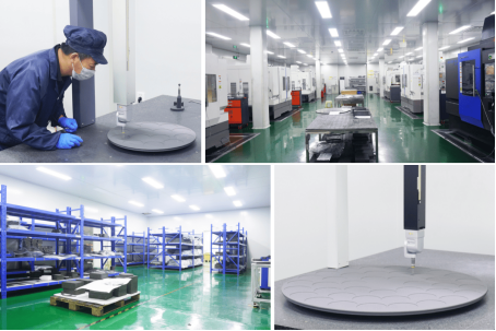
Figure 6: VETEK semiconductor materials production and precision machining base
|
Core Conclusion: Typical sample lead time is as fast as approximately 20 days; actual delivery depends on drawing complexity, materials, coating, quantity, and inspection requirements. |
The typical lead time for customized AMAT hollow lift pin samples is as fast as approximately 20 days. Actual delivery time may vary depending on drawing complexity, material selection, coating requirements, quantity, and inspection requirements. For repeat orders or already qualified products, production schedules can be separately negotiated according to customer forecasts and required delivery dates.
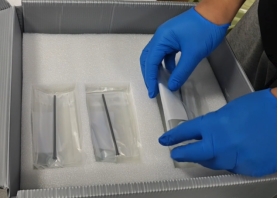
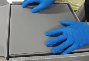
Figure 7: VETEK AMAT hollow lift pin product packaging
|
Core Conclusion: Comprehensive customization capability integrating high-purity graphite procurement and precision machining, CVD silicon carbide coating (including inner wall), and AMAT-compatible solutions into one integrated process. |
VETEK integrates graphite material procurement, precision machining, CVD silicon carbide coating, and semiconductor component manufacturing into an integrated production process. Key capabilities include:
• High-purity graphite substrate (SGL Carbon / Toyo Tanso, etc.)
• CVD silicon carbide coating purity 6N
• Standard coating thickness 100±20 μm
• Hollow structure machining
• Inner-wall CVD silicon carbide coating (core differentiating capability)
• Precision CNC machining
• AMAT-compatible wafer lift pin solutions
• Sample lead time as fast as approximately 20 days
VETEK covers the complete technical chain of CVD equipment development, CVD process development, CNC precision machining, and purification, supported by dedicated R&D centers and semiconductor materials production facilities.
Q1: What is the standard CVD silicon carbide coating thickness of VETEK AMAT hollow lift pins?
The standard coating thickness is approximately 100±20 μm. Specific thickness can be adjusted according to customer drawings and process requirements.
Q2: What purity level can the CVD silicon carbide coating achieve?
Depending on the selected specification, the coating purity is approximately 6N (99.99995%). VETEK's CVD silicon carbide platform routinely operates at the 6N–7N level.
Q3: Why is inner-wall coating critical for hollow lift pins?
The internal geometry is difficult to coat uniformly. High-quality inner-wall silicon carbide coverage prevents the graphite substrate from being exposed to high-temperature, chemically active process environments and is a key differentiating factor for long-term reliability. Inner-wall coating uniformity is directly related to internal bore cleanliness and wafer yield.
Q4: Can VETEK manufacture according to my OEM drawings or samples?
Yes. VETEK can manufacture according to customer drawings, OEM part numbers (such as AMAT 0200-03201), sample components, dimensional specifications, required graphite grade, and coating requirements.
Q5: What is the typical sample lead time?
Typical sample lead time is as fast as approximately 20 days. Actual delivery depends on drawing complexity, material selection, coating requirements, quantity, and inspection needs.
Although the AMAT hollow lift pin is a relatively small semiconductor component, its manufacturing requirements are far from simple. Thin-wall geometry, strict concentricity requirements, high-temperature operation, contamination control, and the combination of inner-surface coating make it a specialized semiconductor process component.
VETEK's current solution adopts high-purity graphite with CVD silicon carbide coating, combining the machinability and thermal characteristics of graphite with the high purity, chemical resistance, and high-temperature stability of CVD silicon carbide. With a standard coating thickness of 100±20 μm, purity up to 6N, SGL and Toyo Tanso graphite material options, and inner-wall coating capability, VETEK can provide customized AMAT hollow lift pin solutions for semiconductor wafer handling and silicon epitaxy applications.
For customers seeking alternative suppliers of AMAT 0200-03201 hollow wafer lift pins, or other silicon carbide coated graphite semiconductor components, VETEK can evaluate drawings or samples and provide customized manufacturing solutions.

-
+86-579-87223657
Wangda Road, Ziyang Street, Wuyi County, Jinhua City, Zhejiang Province, China