

QR Code

Products
Contact Us


Fax
+86-579-87223657

Email

Address
Wangda Road, Ziyang Street, Wuyi County, Jinhua City, Zhejiang Province, China


|
Industry |
Semiconductor manufacturing, advanced ceramics, third-generation semiconductor materials |
|
Process |
Water Jet Guided Laser (WJGL) one-pass through-hole machining |
|
Solution |
Custom 35mm × 2mm SiC substrates with Φ0.15mm precision micro-holes |
|
Services |
Technical consultation, process development, inspection reports, customized coating & machining |
|
Results |
• Uniform hole geometry from inlet to outlet confirmed by SEM • No measurable taper; aspect ratio suitable for 2mm thickness • Minimal heat-affected zone and virtually no chipping on hard-brittle SiC • Successful delivery and customer acceptance for secondary-battery material development |
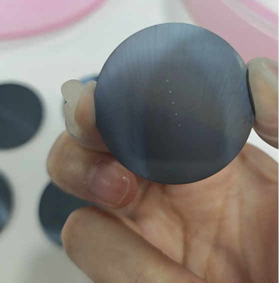
Figure 1:product photo of 35mm × 2mm SiC substrate after water-guided laser micro-hole machining
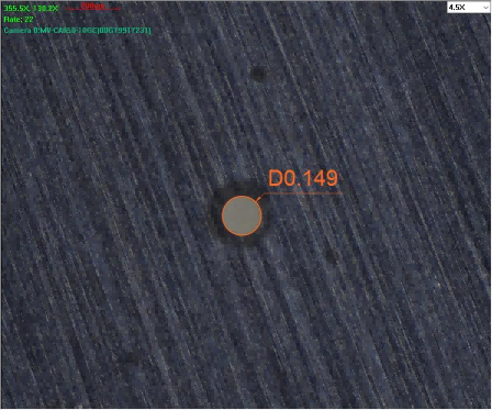
Figure 2:SEM image of VeTek water-guided laser machined Φ0.15mm hole in SiC substrate
VeTek Semiconductor’s water-guided laser (WJGL) technology enables one-pass, taper-free micro-hole machining in thick silicon carbide (SiC) substrates. In a recent project, Φ0.15 mm through-holes were successfully processed on 35 mm diameter × 2 mm thick N-type 4H-SiC substrates. SEM inspection verified highly uniform hole walls from inlet to outlet, meeting stringent semiconductor-grade requirements.
|
Core conclusion: The cylindrical water jet acts as a liquid optical fiber that guides the laser by total internal reflection, producing a parallel energy beam that cuts vertically without the conical kerf typical of conventional lasers. |
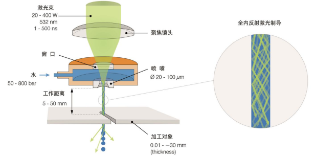
Figure 3: Principle of water-guided laser: laser energy confined by high-pressure water microjet (water optical fiber)
High-pressure water is forced through a precision nozzle (30–120 µm diameter) to form a stable microjet. A focused 532 nm laser is coupled into this jet through a glass window. Once inside the water column, the laser is confined by total internal reflection and travels as a high-energy-density “water optical fiber.” When the microjet contacts the workpiece, the laser ablates the material while the continuous water flow cools the cutting zone and flushes debris.
Because the guiding medium is a cylindrical column of constant diameter, the emerging laser energy remains parallel over a working distance of several tens of millimeters. Consequently, the cut wall stays vertical even on 2 mm (and up to 60 mm) thick SiC, eliminating the need for focus tracking and preventing the taper that appears in free-space laser drilling.
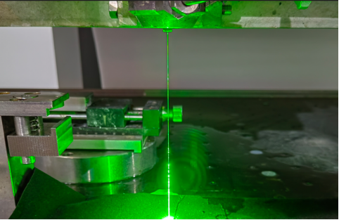
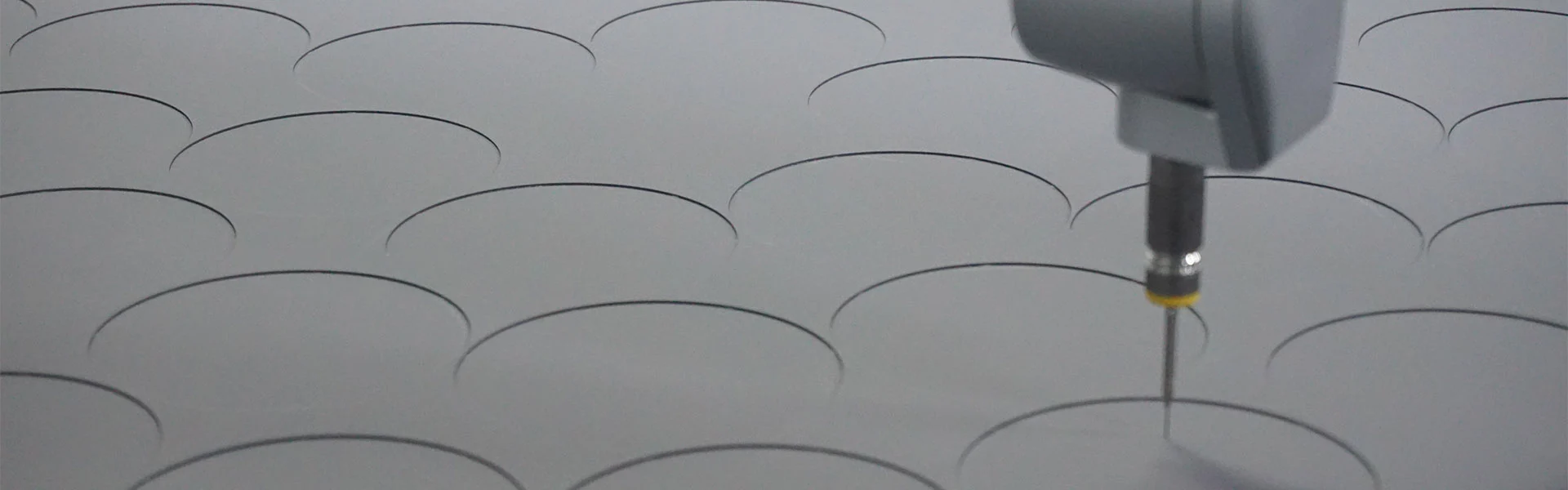
Figure 4: Actual photo of the water-guided laser working scene
• No focus adjustment required for thicknesses up to 60 mm
• Zero or near-zero taper (10–20 µm inlet-to-exit difference)
• Continuous cooling suppresses thermal stress and edge chipping
• Uniform energy distribution across the jet cross-section reduces surface roughness (Ra 0.3–1 µm)
• Kerf width as narrow as 50 µm, minimizing material loss on expensive SiC
|
Core conclusion: WJGL combines the precision of laser ablation with the cooling and cleaning action of a high-pressure water jet, making it uniquely suited to hard, brittle ceramics such as SiC, Si₃N₄, AlN and diamond. |
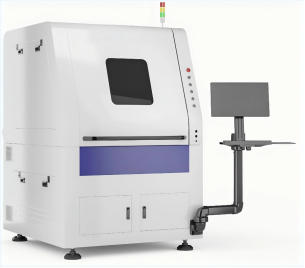
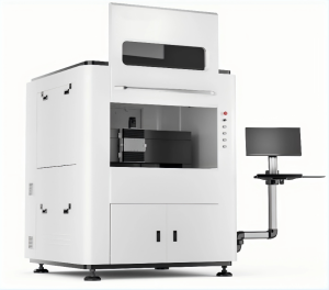
Figure 5. VeTek water-guided laser equipment (WL series)
Traditional mechanical drilling of Φ0.15 mm holes in 2 mm SiC frequently suffers from tool breakage, edge fracture and progressive diameter variation. Free-space laser drilling, while non-contact, generates heat-affected zones, recast layers and noticeable taper. Water-guided laser overcomes both sets of limitations:
1. One-pass through-hole capability – eliminates the alignment errors of double-sided processing.
2. High aspect ratio – ratios exceeding 30:1 are routinely achieved.
3. Ultra-low mechanical force – water jet force is only ~1 N, allowing safe processing of ultra-thin or fragile wafers.
4. Clean, slag-free surfaces – continuous flushing removes debris and prevents redeposition.
|
Core conclusion: Beyond the demonstrated 35 mm × 2 mm SiC substrate with Φ0.15 mm holes, WJGL is applied to ingot coring, wafer dicing, irregular shaping, and precision ceramic components for semiconductor equipment. |
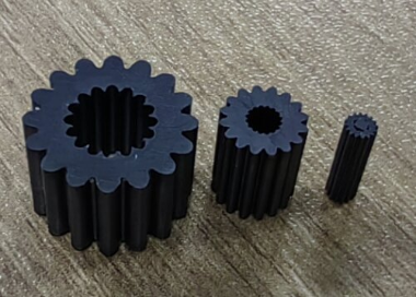
Figure 6. Precision ceramic components processed by water-guided laser
Typical capabilities include:
• Processing thickness range: 0.05–60 mm (SiC, boron carbide ceramics)
• Minimum aperture: 0.1 mm (dependent on thickness)
• Dimensional accuracy: ±0.01 mm
• Surface roughness: 0.3–1 µm
• Equipment platforms: WL-DCS200 (200 × 240 mm work area, 50–60 W) and WL-LCS500 (500 × 500 mm, 100–200 W)
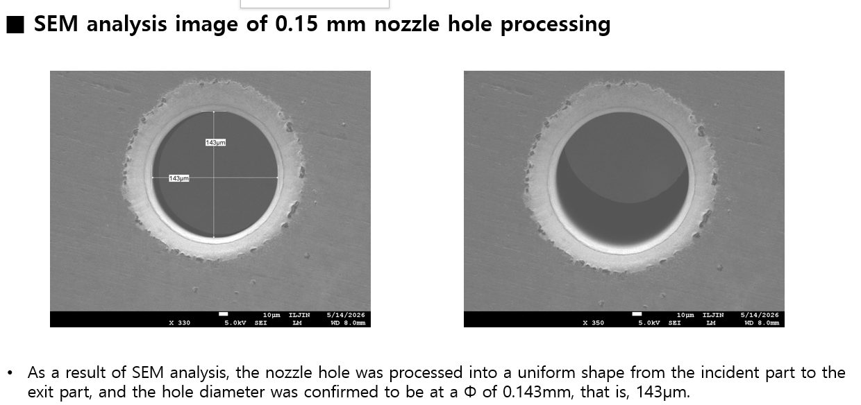
Figure 7.Customer SEM verification of uniform Φ0.15mm through-hole from inlet to outlet in 2mm SiC substrate
In collaboration with a Korean technology partner, VeTek delivered five 35 mm diameter, 2 mm thick N-type 4H-SiC substrates each containing a precision Φ0.15 mm through-hole. SEM analysis performed by the end customer confirmed that the nozzle hole maintained a uniform cylindrical shape from the laser-entry side to the exit side. The parts were accepted for evaluation in silicon-alloy anode material development for next-generation lithium-ion batteries.
Q1: Can water-guided laser process holes smaller than Φ0.15 mm in 2 mm SiC?
A: For apertures significantly below 0.15 mm on 2 mm thickness the technical difficulty rises sharply. Smaller holes (e.g., 0.06 mm) are recommended on thinner substrates (≤0.4 mm) to maintain yield and geometry.
Q2: Is the process truly single-pass?
A: Yes. The water-jet-guided beam propagates through the full thickness in one continuous operation, eliminating the misalignment risk of front-and-back drilling.
Q3: What inspection data can be provided?
A: Dimensional measurement reports, optical and SEM images of the hole cross-section, and surface roughness data are supplied with every batch. Full process videos remain confidential but sample geometry verification is standard.
Water-guided laser technology from VeTek Semiconductor offers a reliable, high-yield route to precision micro-features in hard and brittle semiconductor materials. Whether you require custom SiC substrates with micro-holes, ceramic components for process equipment, or advanced CVD SiC / TaC coatings, our engineering team is ready to support your next project.
Explore our SiC coating solutions for further technical details, or contact us to discuss your specific machining requirements.
+86-579-87223657
Wangda Road, Ziyang Street, Wuyi County, Jinhua City, Zhejiang Province, China