


 Coating (2/2) - VeTek Semiconductor")

 Manufacturing Process")


QR Code

About Us
Products
Contact Us

Phone

Fax
+86-579-87223657

E-mail

Address
Wangda Road, Ziyang Street, Wuyi County, Jinhua City, Zhejiang Province, China


The working principle of VeTek Semiconductor’s Silicon On Insulator Wafer mainly relies on its unique structure and material properties. And SOI wafer consists of three layers: the top layer is a single-crystal silicon device layer, the middle is an insulating Buried OXide (BOX) layer, and the bottom layer is a supporting silicon substrate.
 Structure")
the Structure of Silicon On Insulator Wafers (SOI)
Formation of the insulation layer: Silicon On Insulator Wafer is usually manufactured using Smart Cut™ technology or SIMOX (Separation by IMplanted OXygen) technology. Smart Cut™ technology injects hydrogen ions into the silicon wafer to form a bubble layer, and then bonds the hydrogen-injected wafer to the supporting silicon wafer.
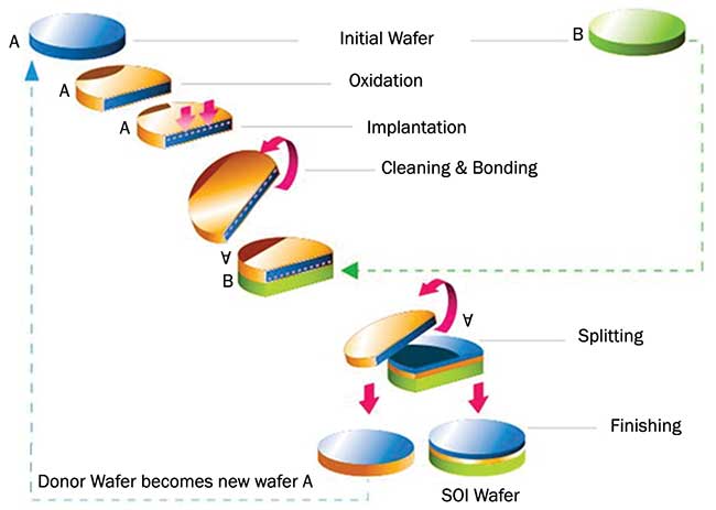
After heat treatment, the hydrogen-injected wafer is split from the bubble layer to form an SOI structure. SIMOX technology implants high-energy oxygen ions into silicon wafers to form a silicon oxide layer at high temperatures.
Reduce parasitic capacitance: The BOX layer of the Silicon carbide Wafer effectively isolates the device layer and the base silicon, significantly reducing parasitic capacitance. This isolation reduces power consumption and increases device speed and performance.
Avoid latch-up effects: The n-well and p-well devices in the SOI wafer are completely isolated, avoiding the latch-up effect in traditional CMOS structures. This allows wafer SOI to be manufactured at higher speeds.
Etch stop function: The single crystal silicon device layer and BOX layer structure of SOI wafer facilitates the manufacturing of MEMS and optoelectronic devices, providing excellent etch stop function.
Through these characteristics, Silicon On Insulator Wafer plays an important role in semiconductor processing and promote the continuous development of the integrated circuit (IC) and microelectromechanical systems (MEMS) industries. We sincerely look forward to further communication and cooperation with you.
The 200mm SOl wafers specification parameter:
|
200 mm SOl wafers specification |
||
|
No |
Description |
Value |
| Device Silicon layer | ||
| 1.1 |
Thickness |
220 nm +/-10 nm |
| 1.2 |
Production method |
CZ |
| 1.3 |
Crystal orientation |
<100> |
| 1.4 | Conductivity type | p |
| 1.5 | Dopant |
Boron |
| 1.6 |
Resistivity average |
8.5 - 11.5 0hm*cm |
| 1.7 |
RMS (2x2 um) |
<0.2 |
| 1.8 |
LPD (Size>0.2um) |
<75 |
| 1.9 |
Large defects larger than 0.8 microns (Area) |
<25 |
| 1.10 |
Edge Chip,Scratch, Crack,Dimple/Pit,Haze,Orange Peel ( visual inspection) |
0 |
| 1.11 |
Bonding voids:visual inspection >0.5mm diameter |
0 |
Silicon On Insulator Wafers Production shops:

Address
Wangda Road, Ziyang Street, Wuyi County, Jinhua City, Zhejiang Province, China
Tel
+86-579-87223657
Wangda Road, Ziyang Street, Wuyi County, Jinhua City, Zhejiang Province, China