



QR Code

Products
Contact Us


Fax
+86-579-87223657

Email

Address
Wangda Road, Ziyang Street, Wuyi County, Jinhua City, Zhejiang Province, China



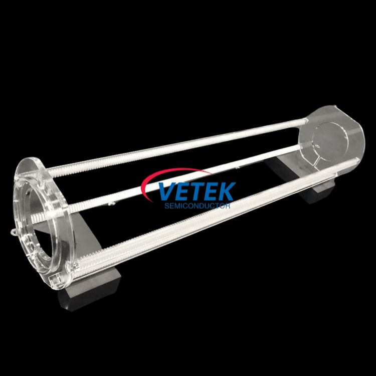
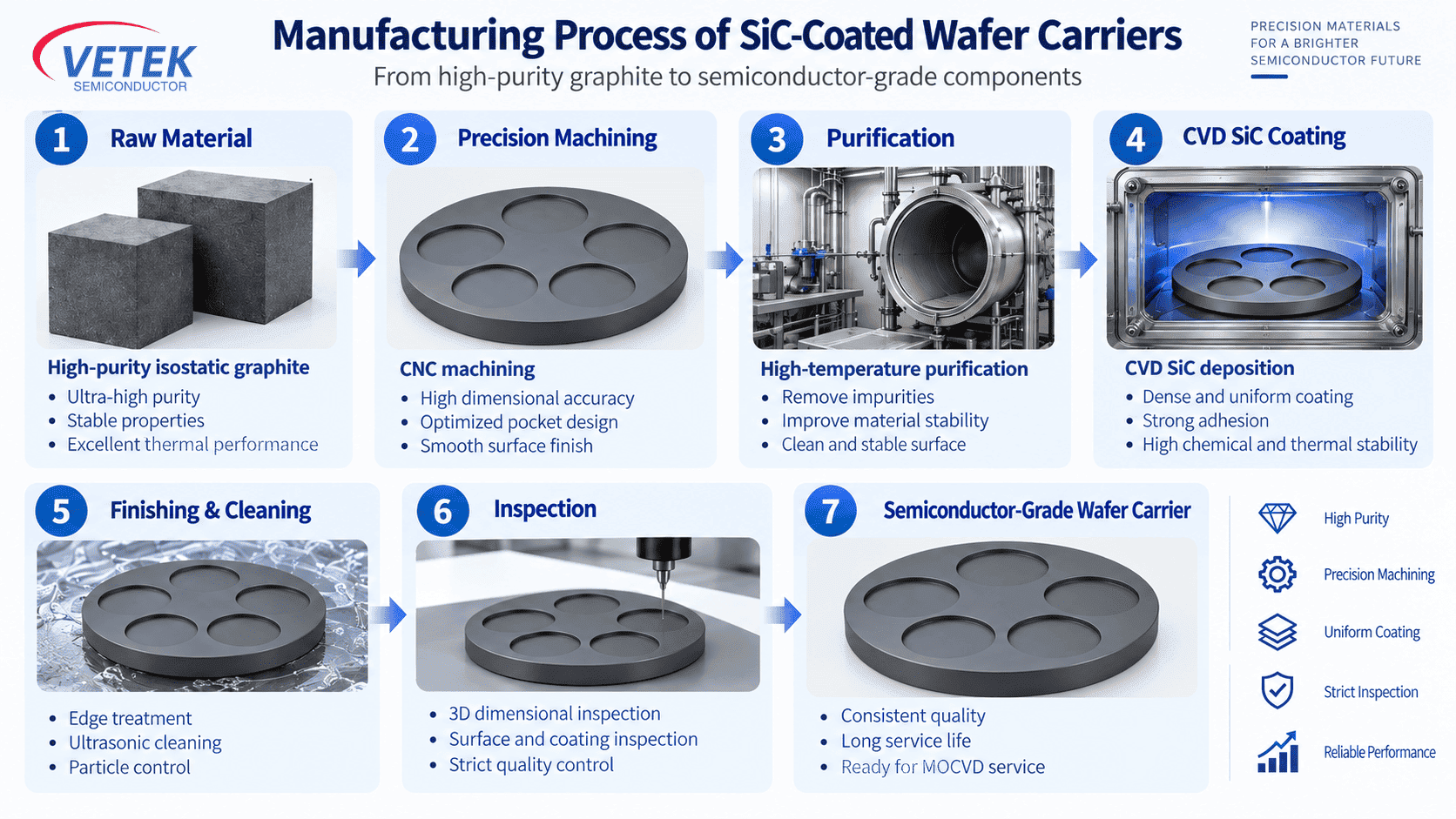
A SiC-coated wafer carrier is one of the key thermal and mechanical interfaces inside an MOCVD reactor. It supports multiple wafers, rotates them through the process environment and helps establish the temperature boundary beneath each substrate. The graphite body provides machinability and thermal functionality, while the CVD silicon carbide coating creates a chemically stable, high-purity process-facing surface.
For GaN and LED epitaxy, the engineering objective is not simply to protect the graphite. The carrier must help maintain consistent wafer temperature, dimensional stability and surface condition over repeated growth and cleaning cycles.
Metal-organic chemical vapor deposition combines gas-phase chemistry, fluid transport and heat transfer in a highly temperature-sensitive epitaxial process. The wafer carrier sits directly beneath the substrates and therefore becomes part of the thermal system that determines the actual wafer-surface temperature.
A simplified relationship is:
Heater / Energy Source → SiC-Coated Wafer Carrier → Wafer Thermal Boundary → Wafer Temperature → Epitaxial Growth
This relationship is particularly important for GaN-based materials. Indium incorporation into InGaN quantum wells is strongly temperature dependent, so spatial temperature differences can contribute to wavelength non-uniformity across LED wafers. Experimental work on MOVPE-grown GaN structures has directly linked wafer bow and surface-temperature distribution with emission-wavelength homogeneity.
The carrier should therefore not be viewed as a passive tray. Its geometry, thermal properties, rotation, pocket design and surface condition interact with the reactor flow and heating system.
SiC-coated graphite wafer carriers as essential components in LED MOCVD and explicitly connects carrier material properties with coating quality, wavelength deviation and manufacturing yield.
For a multi-wafer carrier, thermal uniformity depends on much more than the nominal heater temperature.
Pocket depth, pocket diameter, carrier flatness, local wall thickness, rotational symmetry and the distance between the wafer and the carrier all influence the local thermal boundary. A small geometric difference between pockets can change conduction, radiation and gas-gap heat transfer beneath different wafers.
This means dimensional accuracy is also a thermal specification.
In a simplified form:
→ Pocket Geometry / Flatness
→ Local Thermal Resistance
→ Wafer Temperature
→ Growth Kinetics
The same principle applies across the diameter of the carrier. Wafers near the center and outer radius may experience different combinations of gas velocity, precursor concentration and heat transfer. Computational studies of commercial GaN MOCVD reactors show that fluid flow, heat transfer and species transport all contribute to growth-rate and uniformity differences across different wafer zones.
Rotation helps average some spatial effects, but it does not eliminate poor carrier geometry or an unstable thermal boundary.
A technically qualified wafer carrier therefore requires control of both macroscopic geometry and local pocket geometry.
Graphite remains attractive because it can be precision-machined into large, multi-pocket carrier geometries and can operate in demanding thermal environments. Bare graphite, however, is not an ideal surface for repeated exposure to nitride MOCVD chemistry.
Recent research on CVD-SiC-coated high-purity graphite susceptors notes that graphite can experience oxidation, wear, gas desorption and dust generation at high temperature. In nitride growth, ammonia decomposition products can also contribute to graphite erosion, creating particulate contamination and shortening component life.
The CVD SiC coating provides a dense process-facing surface that helps isolate the graphite from this environment.
Its practical functions include chemical protection, contamination control, reduced exposure of the graphite substrate and improved surface stability during repeated high-temperature operation.
However, the coating must be treated as part of the complete carrier system. Coating thickness alone does not define quality. Thickness uniformity, roughness, pinholes, microstructure, interface integrity and compatibility with the graphite substrate all matter.
A 2026 study of CVD-SiC coatings on graphite susceptors demonstrated that properly optimized coatings remained stable during reported MOCVD cycling at approximately 1100°C GaN growth conditions, with only a small roughness change and no observed interfacial degradation in the reported characterization.
The useful engineering conclusion is not that one coating has a fixed universal lifetime, but that coating structure and interface stability strongly influence how the carrier ages under MOCVD service.
MOCVD growth rate and alloy composition are both sensitive to local process conditions. For LED structures, temperature variation is especially important because the incorporation of indium into InGaN can change with wafer-surface temperature.
This creates the following process chain:
→ Carrier Thermal Behavior
→ Wafer Temperature Distribution
→ Growth Rate / Composition
→ Thickness or Wavelength Uniformity
→ Device Binning and Yield
This chain should be interpreted carefully.
A wafer carrier alone does not determine yield. Gas distribution, precursor chemistry, pressure, reactor design, wafer bow, rotation and growth recipe remain major variables. Nevertheless, the carrier is one of the hardware components that must remain stable if the process is expected to remain repeatable.
SGL Carbon reports that SiC-coated graphite carriers are designed to reduce wavelength deviation and states that high thermal conductivity, dimensional accuracy and coating quality contribute to improved LED wafer output.
Older multi-wafer GaN MOCVD work also demonstrated the importance of achieving a uniform susceptor temperature field, reporting better than ±3°C surface-temperature distribution for the described reactor configuration.
The broader engineering lesson is that temperature uniformity should be evaluated at the wafer level, not only at the heater or reactor set point.
There is no universal number of MOCVD runs after which every SiC-coated wafer carrier should be replaced.
Service life depends on the combined effects of operating temperature, process chemistry, cleaning chemistry, thermal cycling, deposition build-up, coating integrity, handling and dimensional stability.
Typical degradation mechanisms include surface roughening, coating cracking, edge peeling, local delamination, pinholes, deposit accumulation and changes in pocket geometry.
Some of these defects primarily affect mechanical integrity, while others can change the process-facing condition or local thermal behavior before catastrophic failure occurs.
A more useful maintenance question is therefore:
> Has the carrier changed enough to alter wafer temperature, contamination risk or process repeatability?
Depending on the application, inspection can include dimensional checks, flatness measurement, pocket-depth verification, coating-surface inspection and comparison against historical process data.
Cleaning strategy is equally important. Aggressive cleaning may remove deposits but can also accelerate coating degradation if the chemistry or procedure is incompatible with the component.
For this reason, lifetime optimization should focus on stable process performance per service cycle, rather than simply maximizing the number of runs before visible failure.
A technically useful RFQ should begin with the reactor and growth process rather than with a generic request for a “SiC-coated graphite plate.”
The supplier should understand the MOCVD reactor manufacturer and model, wafer material and size, number of pockets, growth chemistry, operating-temperature range, carrier rotation concept and cleaning method.
The drawing should then define pocket diameter, depth, flatness, thickness, edge geometry and other critical tolerances. Graphite purity, CVD SiC coating requirements, surface roughness and inspection methods should be specified around those process requirements.
A practical engineering sequence is:
Reactor → Epitaxy Process → Wafer Layout → Carrier Geometry → Graphite → CVD SiC Coating → Inspection
For replacement carriers, nominal geometry alone may not be sufficient. Qualified graphite grade, coating specification, pocket profile and actual historical process behavior can be equally important.
The objective is to maintain a stable relationship between carrier and wafer over the intended service period:
Dimensional Stability + Thermal Uniformity + Surface Integrity + Low Particle Risk + Repeatable Epitaxy
1. Why are MOCVD wafer carriers made from SiC-coated graphite?
Graphite provides machinability and thermal functionality for complex multi-wafer geometries, while CVD SiC provides a more chemically stable and contamination-resistant process-facing surface.
2. How does a wafer carrier affect MOCVD temperature uniformity?
Carrier flatness, pocket depth, material properties and local geometry influence heat transfer beneath each wafer. These factors interact with reactor heating, gas flow and wafer rotation to determine local wafer temperature.
3. Why is temperature uniformity important for GaN and LED epitaxy?
Growth rate and alloy composition are temperature sensitive. In InGaN-based LED structures, wafer-surface temperature variation can contribute to wavelength variation and therefore influence device binning and process yield.
4. What causes SiC-coated wafer carriers to lose service performance?
Typical causes include coating cracking or delamination, surface roughening, deposit accumulation, thermal cycling, aggressive cleaning, pocket wear and dimensional drift.
5. What information is needed for a custom MOCVD wafer carrier RFQ?
Provide the reactor model, wafer size and material, pocket layout, drawing or STEP file, process temperature, growth and cleaning chemistry, critical dimensions, graphite requirement, SiC coating specification, surface-finish requirement, inspection criteria and quantity.
1. SGL Carbon — Specialty Graphites for LED Chip Production. Technical information on SiC-coated graphite wafer carriers, thermal conductivity, dimensional tolerances, wavelength uniformity and carrier lifetime.
2. Huo, Y. et al. — “Study of the process-structure-property correlation in CVD-SiC coatings on graphite substrates.” Scientific Reports, 2026.
3. Uniformity of the wafer surface temperature during MOVPE growth of GaN-based laser diode structures. Journal of Crystal Growth, 2011.
4. Species transport and chemical reaction in a MOCVD reactor and their influence on GaN growth uniformity. Journal of Crystal Growth, 2016.
+86-579-87223657
Wangda Road, Ziyang Street, Wuyi County, Jinhua City, Zhejiang Province, China