
Products

China Temperatures Above 1,000C Manufacturer, Supplier, Factory

Our pursuit and corporation aim should be to "Always satisfy our consumer requirements". We carry on to build and style and design remarkable quality items for both our outdated and new clients and reach a win-win prospect for our clients at the same time as us for Temperatures Above 1,000C, C/C Composite, Carbon Fiber Reinforced Carbon, High Strength, High Elasticity, Our tenet is "Reasonable price ranges, efficient manufacturing time and finest service" We hope to cooperate with additional consumers for mutual advancement and positive aspects.
Temperatures Above 1,000C, We've got more than 200 staff including experienced managers, creative designers, sophisticated engineers and skilled workers. Through hard work of all employees for the past 20 years own company grew stronger and stronger. We always apply the "client first" principle. We also always fulfill all contracts to the point and therefore enjoy excellent reputation and trust among our customers. You are very welcome to personally visit our company.We hope to start a business partnership on the basis of mutual benefit and successful development . For more information make sure you do no hesitate to contact us.
Hot Products

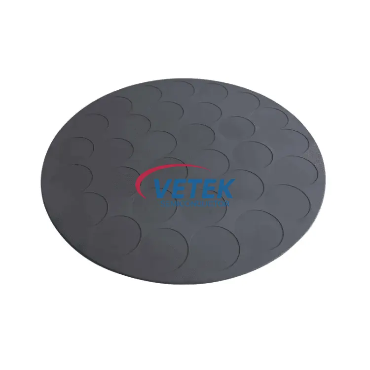
  • MOCVD SiC Coated Susceptor

    MOCVD SiC Coated Susceptor

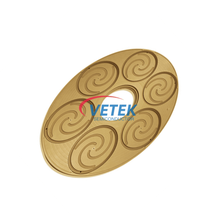
    VETEK MOCVD SiC Coated Susceptor is a precision-engineered carrier solution specifically developed for LED and compound semiconductor epitaxial growth. It demonstrates exceptional thermal uniformity and chemical inertness within complex MOCVD environments. Leveraging VETEK’s rigorous CVD deposition process, we are committed to enhancing wafer growth consistency and extending the service life of core components, providing stable and reliable performance assurance for every batch of your semiconductor production.
  • Physical Vapor Deposition

    Physical Vapor Deposition

    Vetek semiconductor Physical Vapor Deposition (PVD) is an advanced process technology widely used in surface treatment and thin film preparation. PVD technology uses physical methods to directly transform materials from solid or liquid to gas and form a thin film on the surface of the target substrate. This technology has the advantages of high precision, high uniformity and strong adhesion, and is widely used in semiconductors, optical devices, tool coatings and decorative coatings. Welcome to discuss with us!
  • PZT Piezoelectric Wafers (PZT on Si/SOI)

    PZT Piezoelectric Wafers (PZT on Si/SOI)

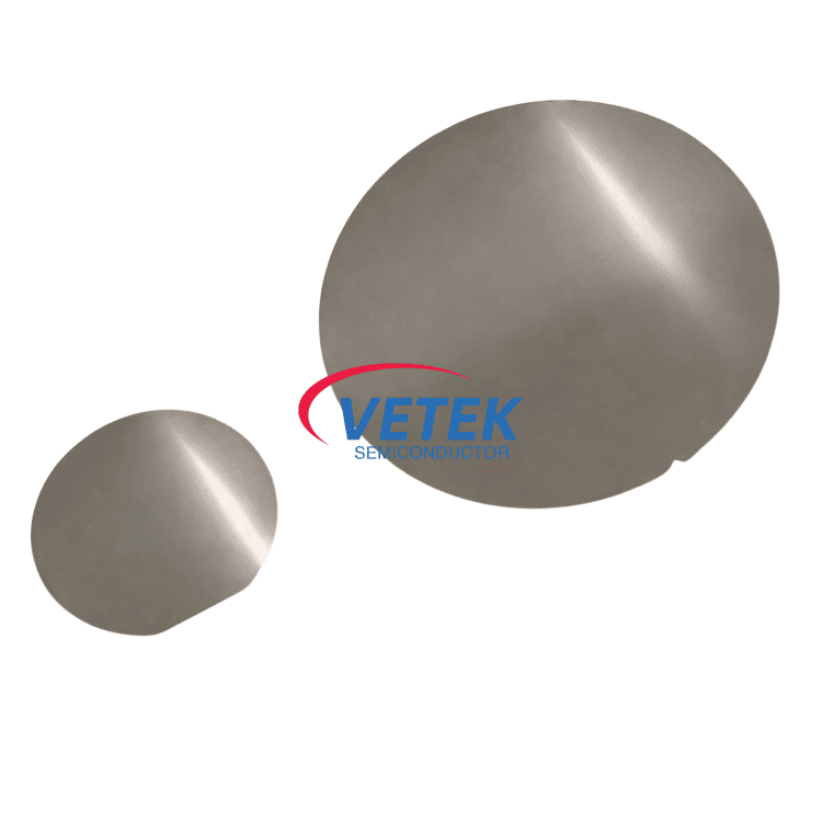
    As the demand for high-sensitivity and low-power MEMS transducers grows with the expansion of 5G communications, precision medical devices, and smart wearables, our PZT on Si/SOI wafers provide a critical material solution. Utilizing advanced thin-film deposition processes such as Sol-gel or sputtering, we achieve exceptional consistency and superior piezoelectric performance on silicon substrates. These wafers serve as the fundamental core for electromechanical energy conversion.
  • SiC Coated Epi Susceptor

    SiC Coated Epi Susceptor

    As the top domestic manufacturer of silicon carbide and tantalum carbide coatings, VeTek Semiconductor is able to provide precision machining and uniform coating of SiC Coated Epi Susceptor, effectively controlling the purity of coating and product below 5ppm. The product life is comparable to that of SGL. Welcome to inquire us.
  • High purity SiC wafer boat carrier

    High purity SiC wafer boat carrier

    VeTek Semiconductor offers customized High purity SiC wafer boat carrier. Made of high purity silicon carbide, it features slots to hold the wafer in place, preventing it from sliding during processing. CVD SiC coating is also available if required. As a professional and strong semiconductor manufacturer and supplier, VeTek Semiconductor's High purity SiC wafer boat carrier is price competitive and high quality. VeTek Semiconductor looks forward to being your long-term partner in China.
  • Focus ring for Etching

    Focus ring for Etching

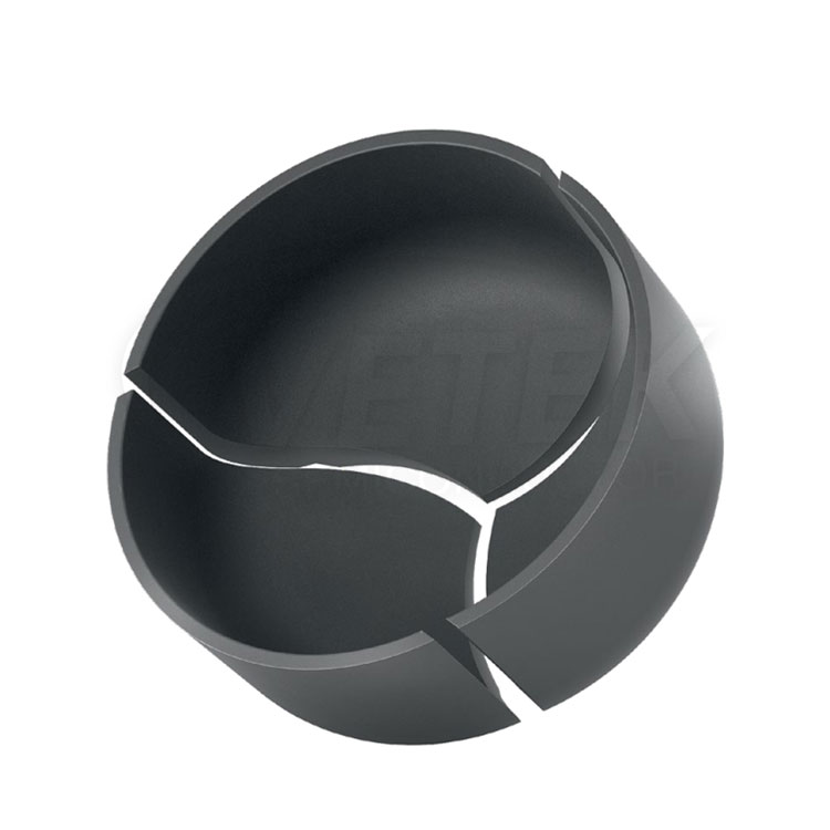
    Focus ring for Etching is the key component to ensure process accuracy and stability. These components are precisely assembled in a vacuum chamber to achieve uniform machining of nanoscale structures on the wafer surface through precise control of plasma distribution, edge temperature and electric field uniformity.

Send Inquiry

X
We use cookies to offer you a better browsing experience, analyze site traffic and personalize content. By using this site, you agree to our use of cookies. Privacy Policy
RejectAccept