


 epitaxy preparation technology")


QR Code

Products
Contact Us


Fax
+86-579-87223657

E-mail

Address
Wangda Road, Ziyang Street, Wuyi County, Jinhua City, Zhejiang Province, China


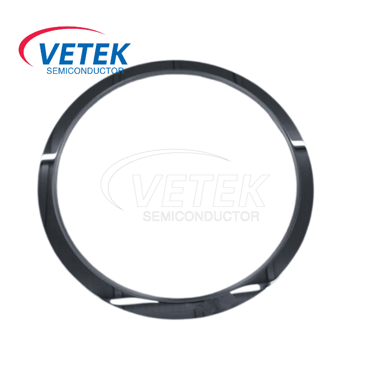
Monocrystalline silicon etching rings are essential components in semiconductor etching processes by maintaining plasma environment stability, protecting equipment and wafers, optimizing resource utilization and adapting to advanced process requirements. Its performance directly affects the yield and cost of chip manufacturing.
The etched Focus Ring, Electrode and ETC (Edge Temperature Controller) are the core consumables to ensure plasma uniformity, temperature control and process repeatability. These components are precisely assembled in the vacuum chamber of the CVD, etching and film equipment and directly determine the accuracy and yield of the etching from edge to center of the wafer.
In response to the stringent demand for material properties in high-end manufacturing processes, Veteksemi innovates by using high-purity Monocrystalline Silicon with a resistivity of 10-20Ω ·cm to manufacture focusing rings and supporting consumables. Through collaborative optimization of material science, electrical design and thermodynamics, VeteKsemi is able to manufacture focusing rings and supporting consumables. Comprehensively surpass traditional Quartz solutions to achieve breakthrough improvements in longevity, accuracy and cost effectiveness.

Monocrystalline silicon VS. Quartz
Project
Monocrystalline silicon focusing ring(10-20 Ω·cm)
Quartz focusing ring
Resistance to plasma corrosion
Life 5000-8000 wafers (fluorine/chlorine based process)
Life span 1500-2000 wafers
Thermal conductivity
149 W/m·K (rapid heat dissipation, ΔT fluctuation ±2℃)
1.4W /m·K (ΔT fluctuation ±10℃)
Coefficient of thermal expansion
2.6×10⁻⁶/K (wafer matched, zero deformation)
0.55×10⁻⁶/K (easy displacement)
Dielectric loss
tanδ <0.001 (accurate electric field control)
tanδ ~0.0001 (electric field distortion)
Surface roughness
Ra <0.1μm (Class 10 cleanliness standard)
Ra <0.5μm (high particle risk)
1. Atomic level process accuracy
Resistivity optimization + ultra-precision polishing (Ra <0.1μm) eliminates micro-discharge and particle contamination to meet SEMI F47 standards.
The dielectric loss (tanδ <0.001) is highly matched to the wafer dielectric environment, avoiding edge electric field distortion and supporting 3D NAND 89.5°±0.3° vertical deep hole etching.
2. Intelligent system compatibility
Integrated with ETC edge temperature control module, the cooling air flow is dynamically adjusted by thermocouple and AI algorithm to compensate chamber thermal drift.
Support customized RF matching network, suitable for mainstream machines such as AMAT Centura, Lam Research Kiyo and ICP/CCP plasma sources.
3. Comprehensive cost-effectiveness
The life of monocrystalline silicon is 275% longer than that of quartz, the maintenance cycle is more than 3,000 hours, and the comprehensive cost of ownership (TCO) is reduced by 30%.
Resistivity gradient customization service (5-100Ω ·cm), precisely matching the customer process window (such as GaN/SiC wide band gap material etching).
Project
Monocrystalline silicon focusing ring(10-20 Ω·cm)
High resistance monocrystalline silicon(>50 Ω·cm)
Quartz focusing ring
Purity
>99.9999%
>99.9999%
>99.99%
Corrosion life (wafer count)
5000-8000
3000-5000
1500-2000
Thermal shock stability
ΔT>500℃/s
ΔT>300℃/s
ΔT<200℃/s
Leakage current density
<1 μA/cm²
/
/
The wafer yield is increased to
+1.2%~1.8%
+0.3%~0.7%
Base value
|
Minimum Order Quantity |
1 set |
|
Price |
Contact for Customized Quotation |
|
Packaging Details |
Standard export package |
|
Delivery Time |
Delivery Time: 30-35 Days After Order Confirmation |
|
Payment Terms |
T/T |
|
Supply Ability |
600 sets/Month |

Address
Wangda Road, Ziyang Street, Wuyi County, Jinhua City, Zhejiang Province, China
Tel
+86-579-87223657
Wangda Road, Ziyang Street, Wuyi County, Jinhua City, Zhejiang Province, China