
Products

China Semiconductor manufacturing fixtures Manufacturer, Supplier, Factory

"Sincerity, Innovation, Rigorousness, and Efficiency" could be the persistent conception of our organization for your long-term to establish alongside one another with shoppers for mutual reciprocity and mutual benefit for Semiconductor manufacturing fixtures, Silicon single crystal puller fixtures, Single crystal growth crucibles, Semiconductor crystal growth fixtures, silicon crystal growth, As a key business of this industry, our company makes endeavours to become a leading supplier, based on the faith of specialist quality & throughout the world company.
Semiconductor manufacturing fixtures, They're durable modeling and promoting well all over the world. Under no circumstances disappearing key functions in a brief time, it's a need to for you personally of fantastic quality. Guided by the principle of Prudence, Efficiency, Union and Innovation. the business make an awesome efforts to expand its international trade, raise its enterprise. rofit and improve its export scale. We've been confident that we will have a vibrant prospect and to be distributed all over the world in the years to come.
Hot Products

  • CVD SiC Coated Barrel Susceptor

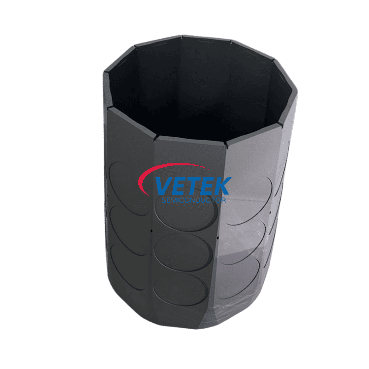
    CVD SiC Coated Barrel Susceptor

    VeTek Semiconductor is a leading manufacturer and innovator of CVD SiC Coated graphite Susceptor in China. Our CVD SiC Coated Barrel Susceptor plays a key role in promoting the epitaxial growth of semiconductor materials on wafers with its excellent product characteristics. Welcome to your further consultation.
  • TaC Coated Guide Ring

    TaC Coated Guide Ring

    TaC Coated Guide Ring is made of high-quality graphite and TaC coating. In the preparation of SiC crystals by PVT method, VeTek Semiconductor's TaC coated guide ring is mainly used to guide and control the airflow, optimize the single crystal growth process, and improve the single crystal yield. With excellent TaC coating technology, our products have excellent high temperature resistance, corrosion resistance and good mechanical properties.
  • Semiconductor grade Quartz Bell Jar

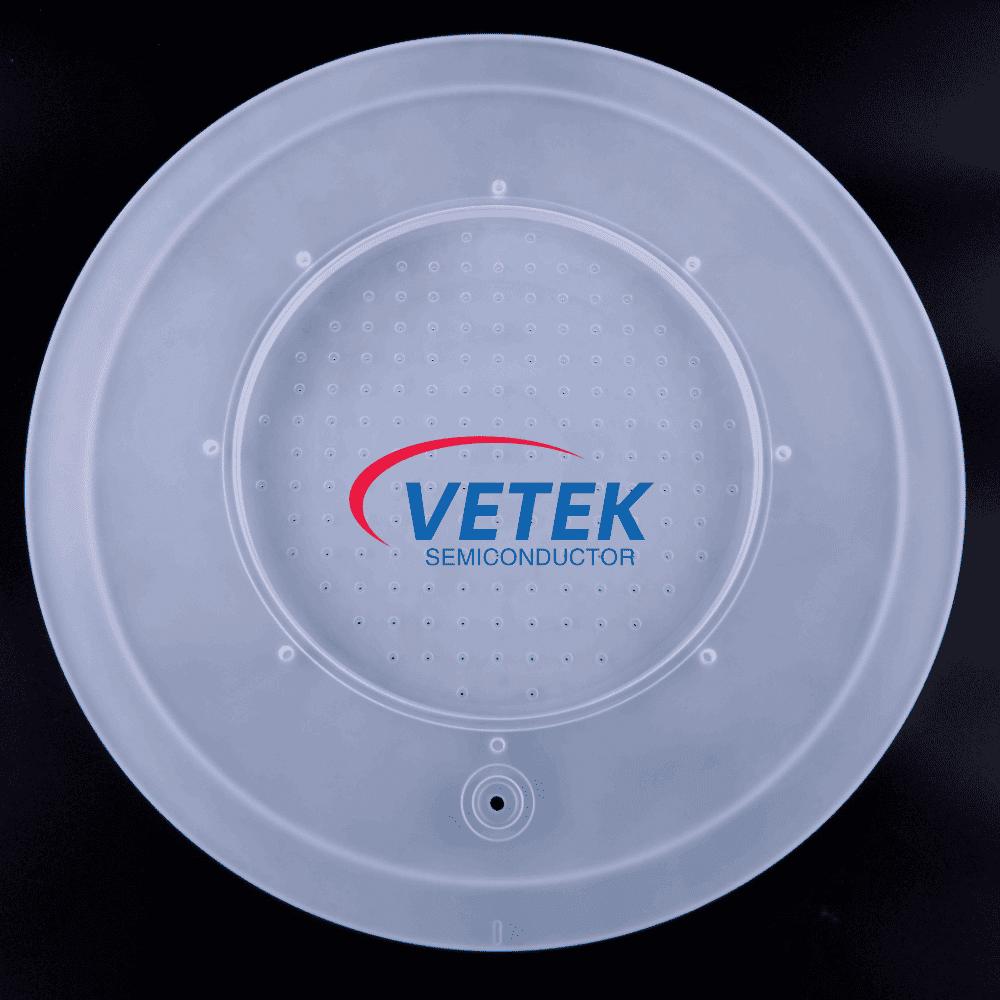
    Semiconductor grade Quartz Bell Jar

    Semiconductor grade Quartz Bell Jar is an important equipment component mainly used in high temperature, high pressure and high purity environments. It is made of high purity quartz material, has excellent thermal stability, chemical resistance and optical transparency, and is widely used in industrial fields such as semiconductor manufacturing and LED production. VeTek Semiconductor has many years of process accumulation in Semiconductor grade Quartz Bell Jar and can provide customized products according to customer needs. Looking forward to your inquiry.
  • PG (Pyrolytic Graphite) Coated Ring

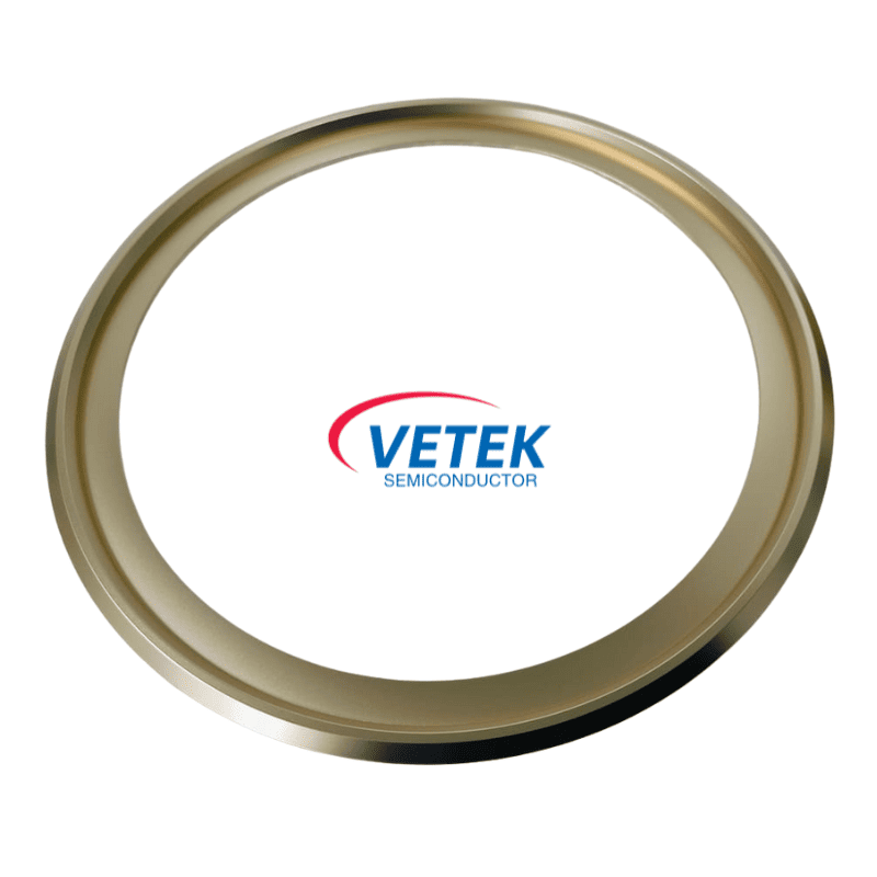
    PG (Pyrolytic Graphite) Coated Ring

    The VETEK PG (Pyrolytic Graphite) Coated Ring is purpose-built for semiconductor thermal field and crystal growth environments where uniform heat distribution and stable temperatures are non-negotiable. Starting with a high-purity graphite base and finished with a dense Pyrolytic Graphite coating, this component delivers exceptional thermal conductivity, stands up to severe thermal shock, and retains its dimensions over long runs at extreme temperatures. You will find these rings used extensively in crystal growth furnaces, high-temperature ovens, and thermal field assemblies for semiconductors—anywhere that precise temperature control directly drives process repeatability and final product quality.
  • SiC Coated Top Plate for LPE PE2061S

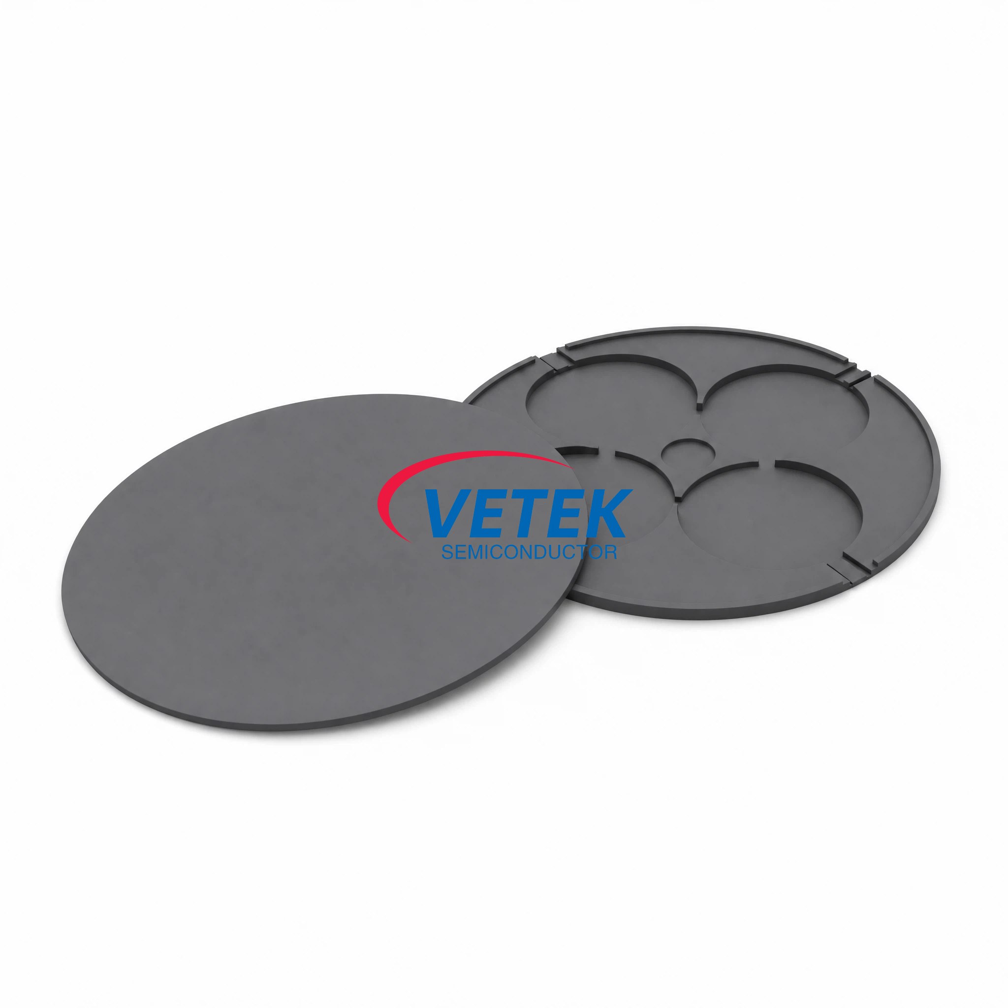
    SiC Coated Top Plate for LPE PE2061S

    VeTek Semiconductor has been deeply engaged in SiC coating products for many years and has become a leading manufacturer and supplier of SiC Coated Top Plate for LPE PE2061S in China. The SiC Coated Top Plate for LPE PE2061S we provide is designed for LPE silicon epitaxial reactors and is located on the top together with the barrel base. This SiC Coated Top Plate for LPE PE2061S has excellent characteristics such as high purity, excellent thermal stability and uniformity, which helps to grow high-quality epitaxial layers. No matter what product you need, we look forward to your inquiry.
  • Wafer Chuck

    Wafer Chuck

    Wafer chunk a wafer clamping tool in semiconductor process and is widely used in PVD, CVD, ETCH and other process.Vetek Semiconductor's wafer chuck play pivotal roles in semiconductor production, enabling fast, high-quality output. With in-house manufacturing, competitive pricing, and robust R&D support, Vetek Semiconductor excels in OEM/ODM services for precision components.Looking forward to your inquiry.

Send Inquiry

X
We use cookies to offer you a better browsing experience, analyze site traffic and personalize content. By using this site, you agree to our use of cookies.Privacy Policy
RejectAccept