Products

China silicon crystal growth Manufacturer, Supplier, Factory

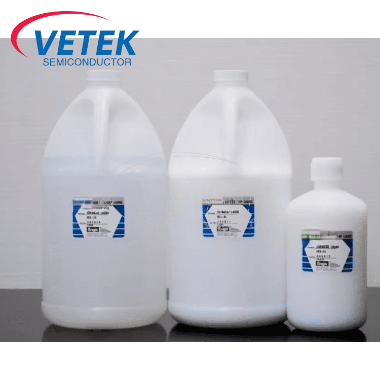
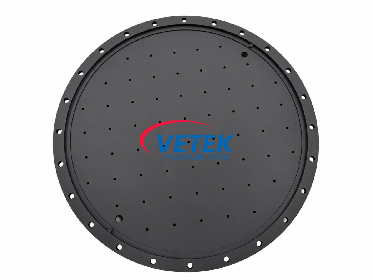
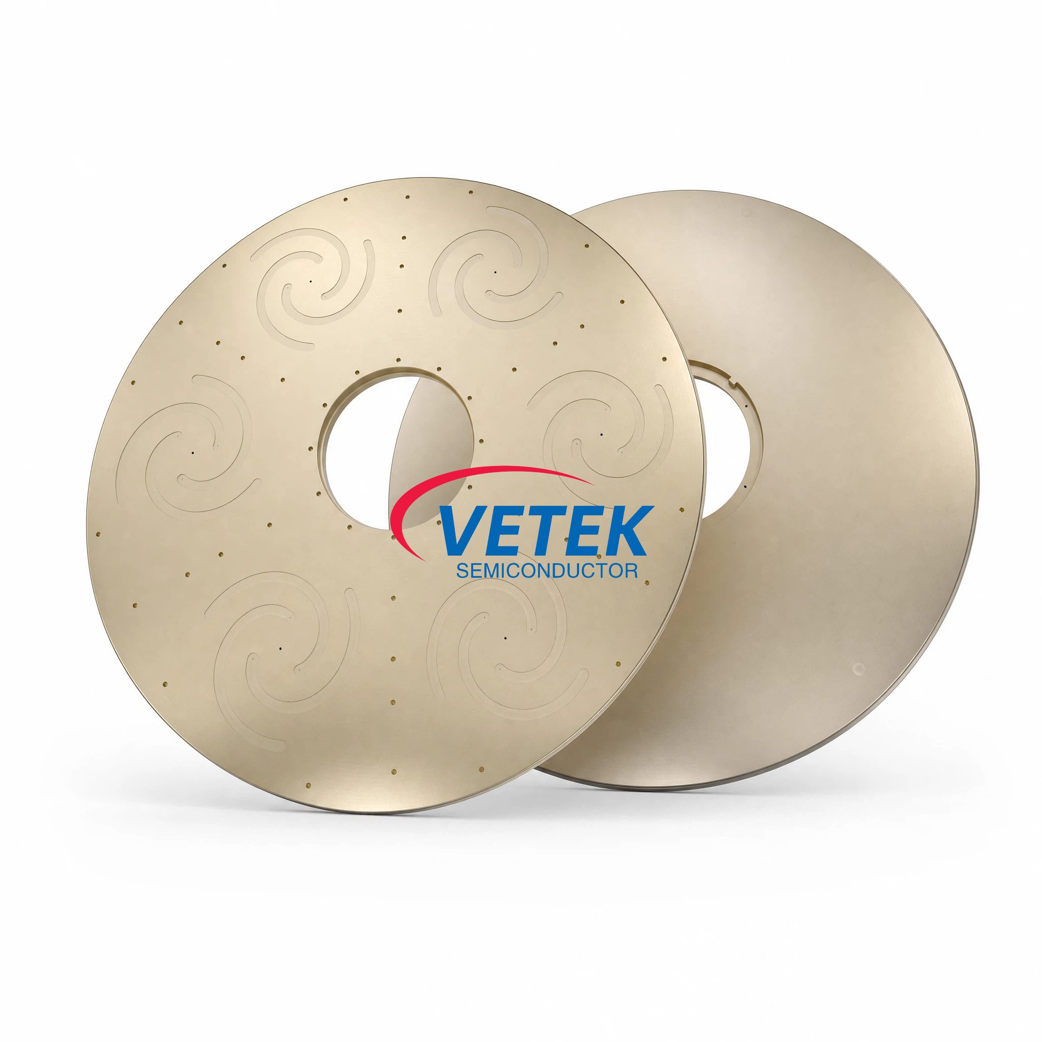
We've got a remarkably efficient crew to deal with inquiries from clients. Our aim is "100% purchaser satisfaction by our item high-quality, selling price & our crew service" and appreciate an excellent popularity amid consumers. With quite a few factories, we could present a wide variety of silicon crystal growth, Silicon single crystal puller fixtures, Single crystal growth crucibles, Semiconductor crystal growth fixtures, High-temperature silicon puller, As an experienced group we also accept tailored orders. The main aim of our corporation is always to develop a satisfying memory for all shoppers, and set up a long-term win-win business partnership.
silicon crystal growth, We sincerely hope to cooperate with customers all over the world, if you would like to have more information, make sure you kindly contact us, we have been looking forward to building up a great business relationship with you.

Hot Products

  • Three-petal Graphite Crucible

    Three-petal Graphite Crucible

    VeTek Semiconductor's Three-petal Graphite Crucible is made of high purity graphite material processed by surface pyrolytic carbon coating, which is used to pull single crystal thermal field. Compared with traditional crucible, the structure of three-lobe design is more convenient to install and disassemble, improve work efficiency, and the impurities below 5ppm can meet the application of semiconductor and photovoltaic industry.
  • Silicon Carbide Robot Arm

    Silicon Carbide Robot Arm

    Our silicon carbide (SiC) robotic arm is designed for high-performance wafer handling in advanced semiconductor manufacturing. Made of high-purity silicon carbide, this robotic arm offers exceptional resistance to high temperatures, plasma corrosion, and chemical attack, ensuring reliable operation in demanding cleanroom environments. Its exceptional mechanical strength and dimensional stability enable precise wafer handling while minimizing contamination risks, making it an ideal choice for MOCVD, epitaxy, ion implantation, and other critical wafer handling applications. We welcome your inquiries.
  • Tantalum Carbide Coated Planetary Rotation Disk

    Tantalum Carbide Coated Planetary Rotation Disk

    VeTek Semiconductor is a leading manufacturer and supplier of Tantalum Carbide Coated Planetary Rotation Disk in China, focusing on TaC coating technology for many years. Our products have high purity and excellent high temperature resistance, which are widely recognized by semiconductor manufacturers. VeTek Semiconductor Tantalum Carbide Coated Planetary Rotation Disk has become the backbone of the wafer epitaxy industry. We look forward to establishing a long-term partnership with you to jointly promote technological progress and production optimization.
  • SiC Coated Silicon Carbide Wafer Boat

    SiC Coated Silicon Carbide Wafer Boat

    SiC Coated Silicon Carbide Wafer Boat is designed with 165 slots to carry wafers.VeTek Semiconductor is professional manufacturer and supplier in China for SiC coated silicon carbide wafer boat, with years of experience in R&D and production, can control the quality well and offer a competitive price. Welcome for visiting our factory and have further discussion on cooperation.
  • Quartz bell jar

    Quartz bell jar

    Vetek Semiconductor is a professional Semiconductor Quartz Bell Jar manufacturer and supplier in China. Our Semiconductor Quartz Bell Jar is widely used in key components of semiconductor manufacturing equipment, especially in CVD, diffusion, oxidation and PVD processes. Vetek Semiconductor is committed to providing advanced Semiconductor Quartz Bell Jar products and technical solutions for the semiconductor industry. Welcome your further inquiries.
  • Alumina Ceramic Vacuum Chuck

    Alumina Ceramic Vacuum Chuck

    VeTek Semiconductor is a professional Alumina Ceramic Vacuum Chuck manufacturer and factory in China. Alumina Ceramic Vacuum Chuck uses high-purity aluminum oxide ceramics with excellent heat resistance, chemical resistance and mechanical strength. It is mainly used to fix and support wafers and substrates. It is a high-performance equipment for semiconductor processing. Welcome your further inquiries.

Send Inquiry

X
We use cookies to offer you a better browsing experience, analyze site traffic and personalize content. By using this site, you agree to our use of cookies. Privacy Policy
Reject Accept