
Products

China LED Epitaxy Manufacturer, Supplier, Factory

We always think and practice corresponding to the change of circumstance, and grow up. We goal at the achievement of a richer mind and body and also the living for LED Epitaxy, CVD SiC, Silicon Carbide, Etching Ring, Bulk SiC, Make sure you sense absolutely absolutely free to speak to us for organization. nd we believe we are going to share the ideal trading practical experience with all our merchants.
LED Epitaxy, With high quality, reasonable price, on-time delivery and customized & customized services to help customers achieve their goals successfully, our company has got praise in both domestic and foreign markets. Buyers are welcome to contact us.
Hot Products

  • Silicon Carbide Robot Arm

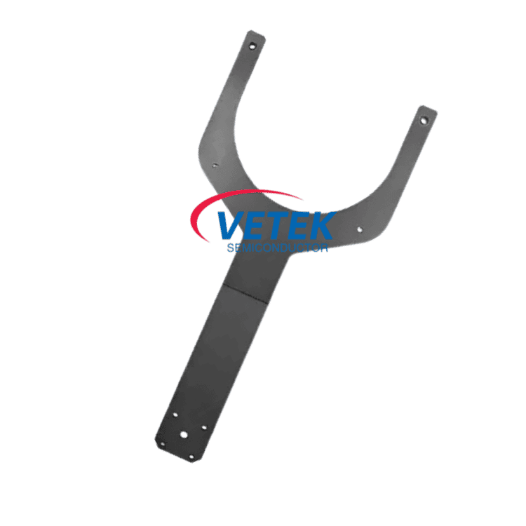
    Silicon Carbide Robot Arm

    Our silicon carbide (SiC) robotic arm is designed for high-performance wafer handling in advanced semiconductor manufacturing. Made of high-purity silicon carbide, this robotic arm offers exceptional resistance to high temperatures, plasma corrosion, and chemical attack, ensuring reliable operation in demanding cleanroom environments. Its exceptional mechanical strength and dimensional stability enable precise wafer handling while minimizing contamination risks, making it an ideal choice for MOCVD, epitaxy, ion implantation, and other critical wafer handling applications. We welcome your inquiries.
  • PSS Etching Carrier Plate for Semiconductor

    PSS Etching Carrier Plate for Semiconductor

    VeTek Semiconductor's PSS Etching Carrier Plate for Semiconductor is a high-quality, ultra-pure graphite carrier designed for wafer handling processes. Our carriers have excellent performance and can perform well in harsh environments, high temperatures and harsh chemical cleaning conditions. Our products are widely used in many European and American markets, and we look forward to becoming your long-term partner in China.You are welcome to come to China to visit our factory and learn more about our technology and products.
  • High purity Rigid felt tube

    High purity Rigid felt tube

    VeTek Semiconductor high purity rigid felt tubes are the first choice for high-temperature applications in the semiconductor industry. Their high compressive strength and excellent thermal insulation properties make them reliable and efficient components in the crystal growth process. VeTek Semiconductor has always been committed to providing advanced and reliable high-purity rigid felt tube technology and product solutions for the semiconductor industry. We welcome your further inquiries.
  • Silicon Carbide Shower Head

    Silicon Carbide Shower Head

    Silicon Carbide Shower Head has excellent high temperature tolerance, chemical stability, thermal conductivity and good gas distribution performance, which can achieve uniform gas distribution and improve film quality. Therefore, it is usually used in high temperature processes such as chemical vapor deposition (CVD) or physical vapor deposition (PVD) processes. Welcome your further consultation to us ,vetek semiconductor.
  • CVD TaC Coating Crucible

    CVD TaC Coating Crucible

    VeTek Semiconductor is a professional manufacturer and leader of CVD TaC Coating Crucible products in China. CVD TaC Coating Crucible is based on tantalum carbon (TaC) coating. The tantalum carbon coating is evenly covered on the surface of the crucible through chemical vapor deposition (CVD) process to enhance its heat resistance and corrosion resistance. It is a material tool specially used in high temperature extreme environments. Welcome your further consultation.
  • Silicon Carbide Seal Ring

    Silicon Carbide Seal Ring

    As a professional Silicon Carbide Seal Ring product manufacturer and factory in China, VeTek Semiconductor Silicon Carbide Seal Ring is widely used in semiconductor processing equipment due to its excellent heat resistance, corrosion resistance, mechanical strength and thermal conductivity. It is especially suitable for processes involving high temperature and reactive gases such as CVD, PVD and plasma etching, and is a key material choice in the semiconductor manufacturing process. Your further inquiries are welcome.

Send Inquiry

X
We use cookies to offer you a better browsing experience, analyze site traffic and personalize content. By using this site, you agree to our use of cookies. Privacy Policy
RejectAccept