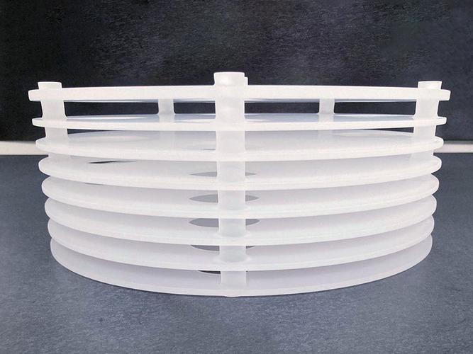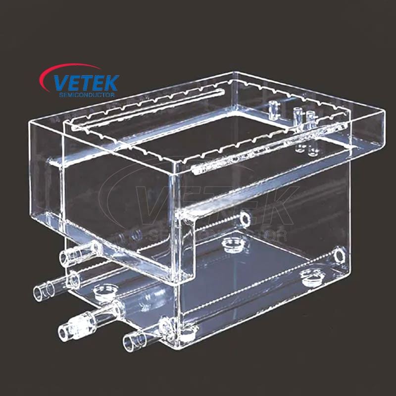
In the ever-evolving world of home and kitchen appliances, one product has recently gained significant attention for its innovation and practical application—the Quartz Thermos Bucket
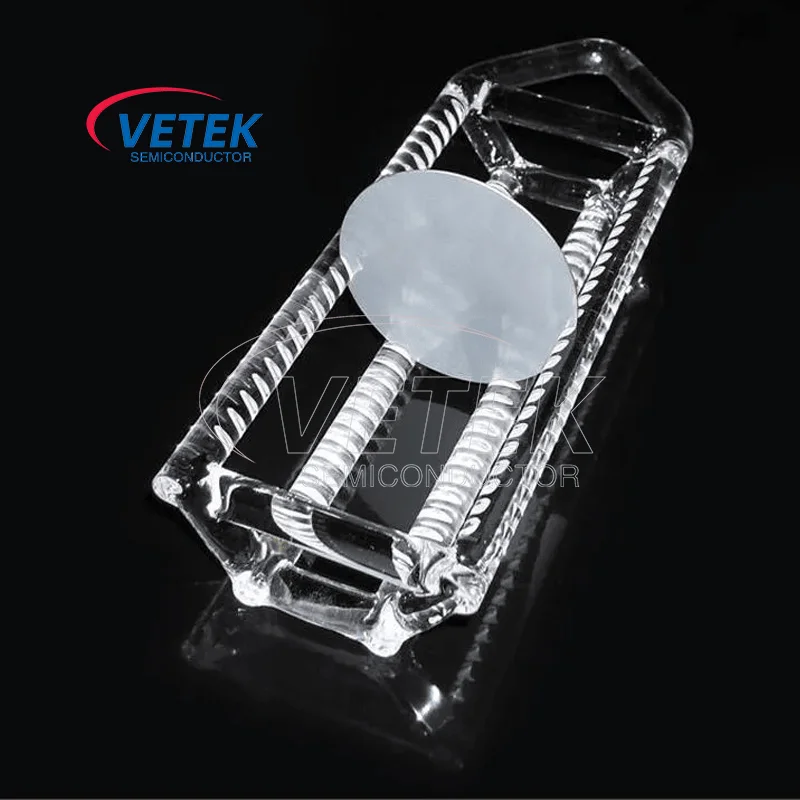
Quartz products are widely used in the semiconductor manufacturing process due to their high purity, high-temperature resistance, and strong chemical stability.
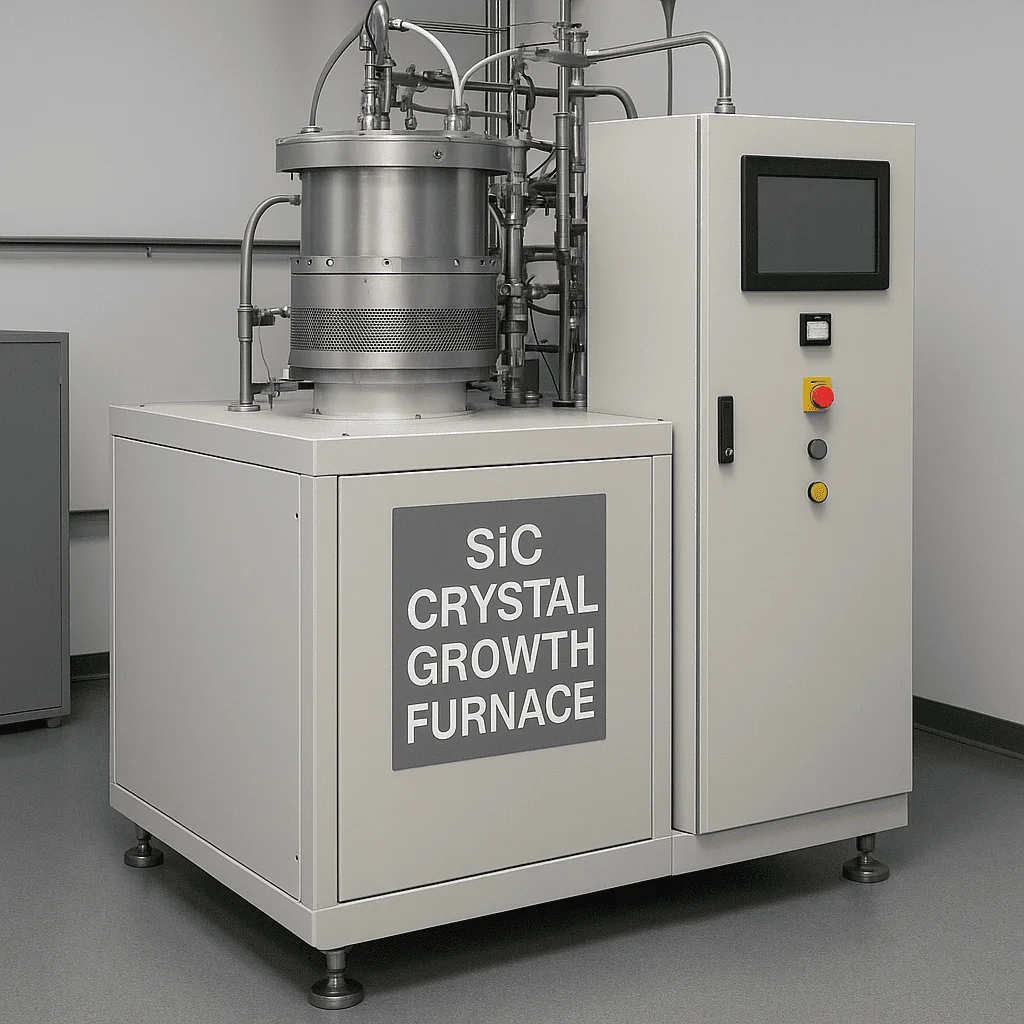
Silicon carbide (SiC) crystal growth furnaces play a vital role in producing high-performance Sic wafers for next-generation semiconductor devices. However, the process of growing high-quality SiC crystals presents significant challenges. From managing extreme thermal gradients to reducing crystal defects, ensuring uniform growth, and controlling production costs, each step requires advanced engineering solutions. This article will analyze the technical challenges of SIC crystal growth furnaces from multiple perspectives.
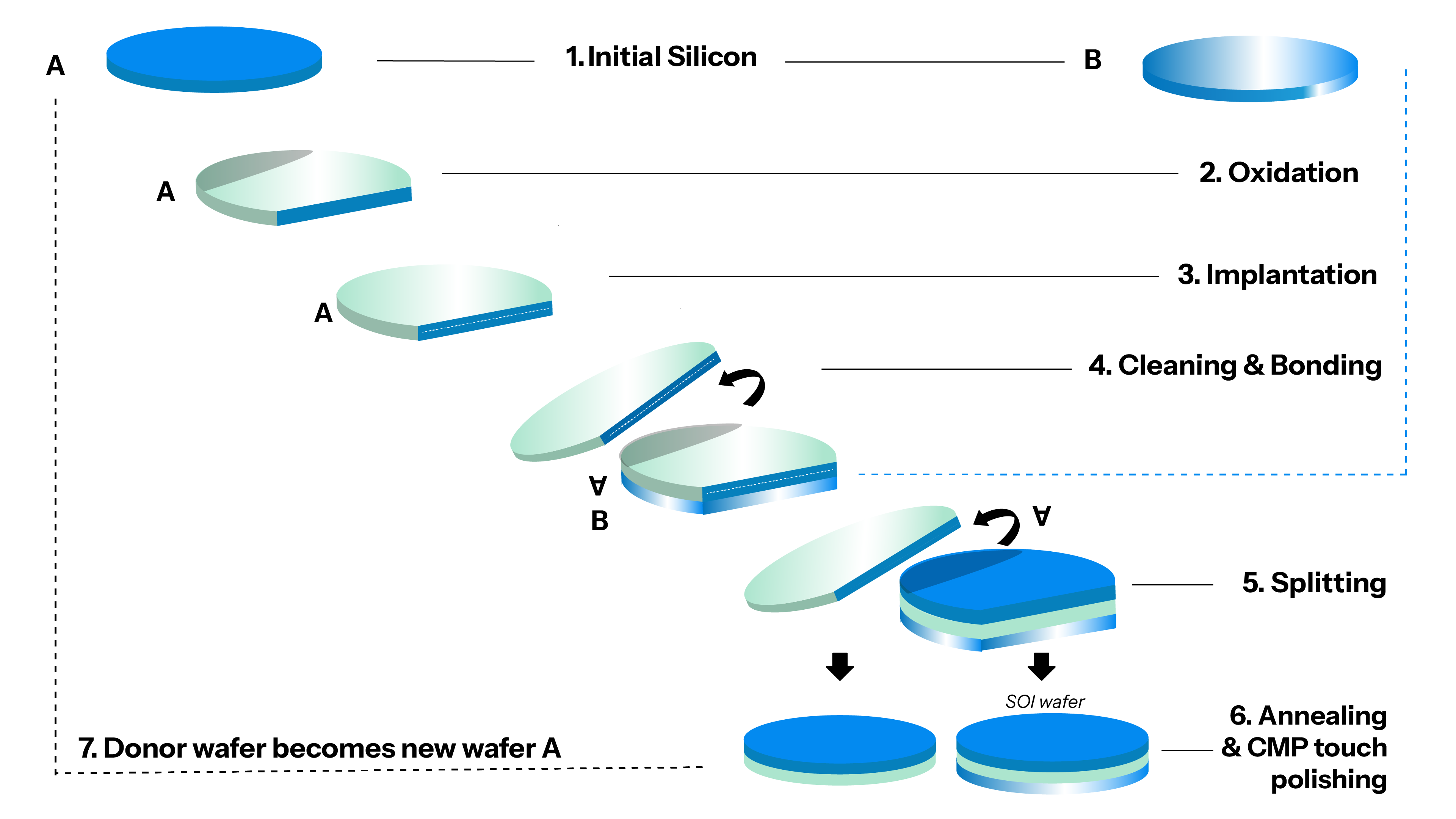
Smart cut is an advanced semiconductor manufacturing process based on ion implantation and wafer stripping, specifically designed for the production of ultra-thin and highly uniform 3C-SiC (cubic silicon carbide) wafers. It can transfer ultra-thin crystal materials from one substrate to another, thereby breaking the original physical limitations and changing the entire substrate industry.
In the preparation of high-quality and high-yield silicon carbide substrates, the core requires precise control of production temperature by good thermal field materials. Currently, the thermal field crucible kits mainly used are high-purity graphite structural components, whose functions are to heat molten carbon powder and silicon powder as well as to maintain heat.
When you see the third-generation semiconductors, you will surely wonder what the first and second generations were. The "generation" here is classified based on the materials used in semiconductor manufacturing.
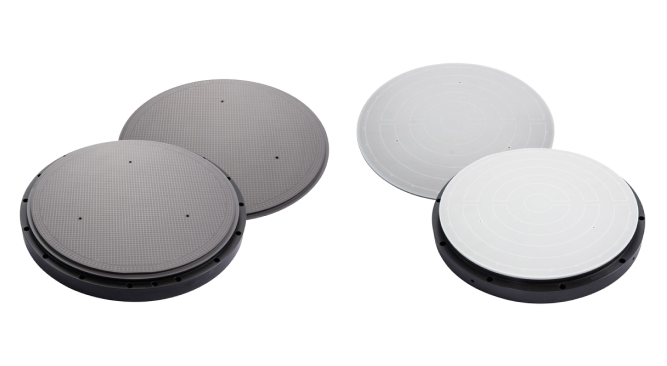
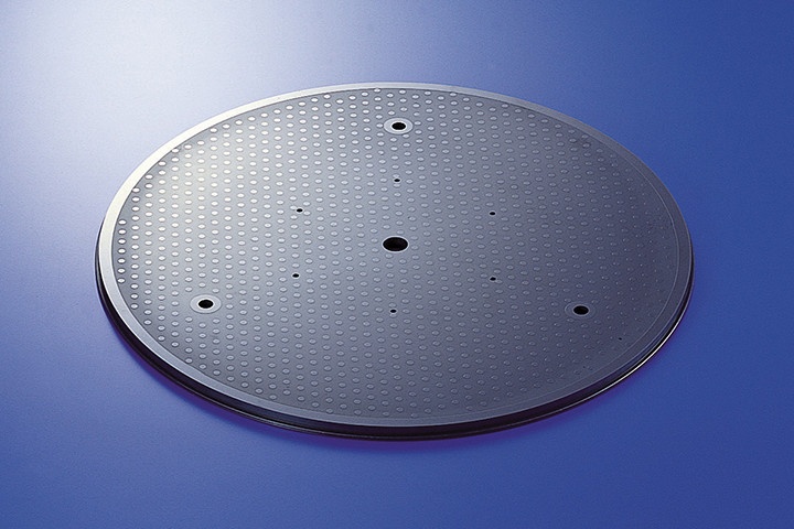
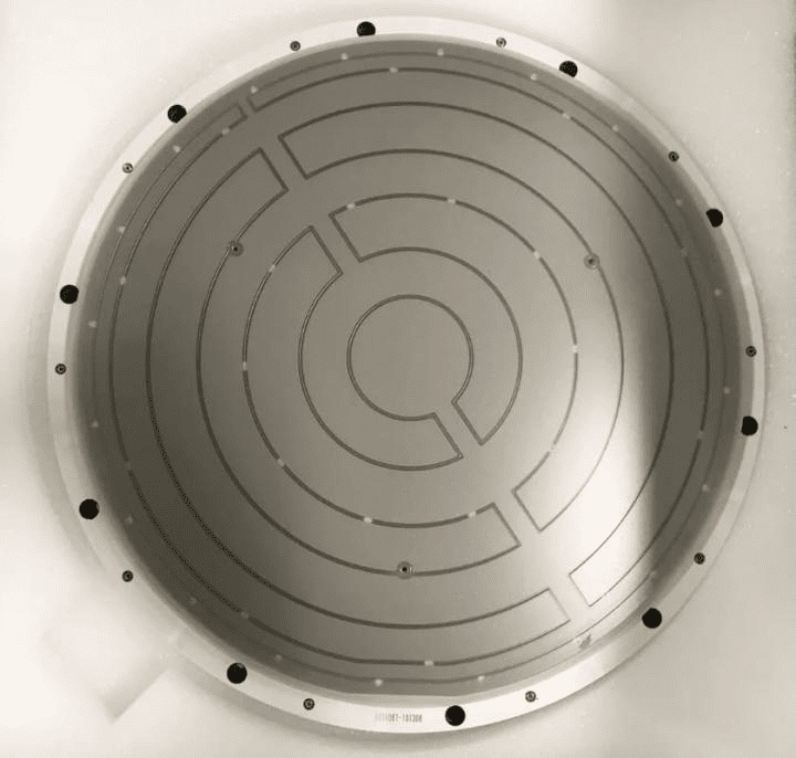
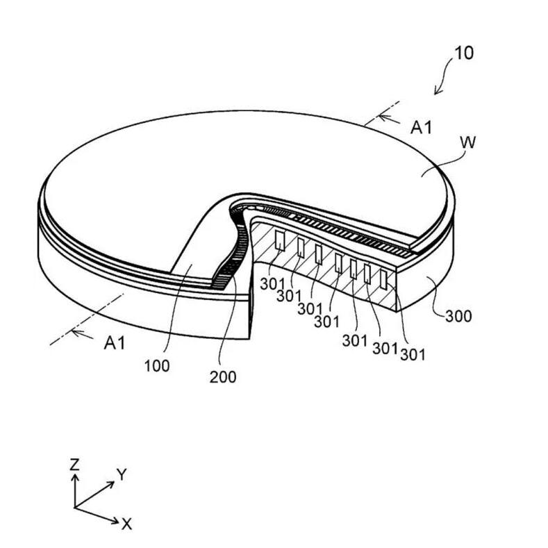
The electrostatic chuck(ESC), also known as the electrostatic chuck (ESC, e-chuck), is a fixture that uses the principle of electrostatic adsorption to hold and fix the adsorbed material. It is suitable for vacuum and plasma environments.
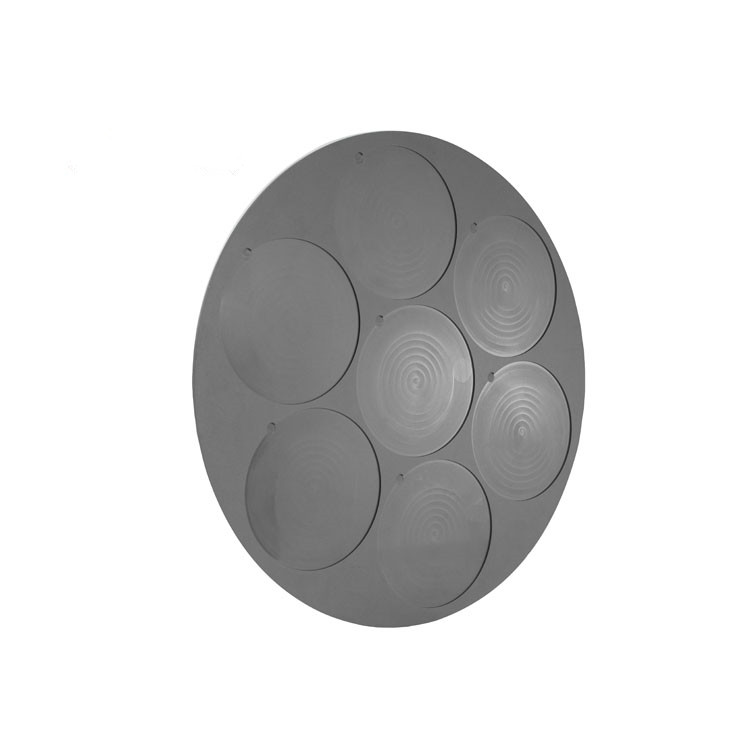
SiC wafer carriers, as key consumables in the third-generation semiconductor industry chain, their technical characteristics directly affect the yield of epitaxial growth and device manufacturing. With the surging demand for high-voltage and high-temperature devices in industries such as 5G base stations and new energy vehicles, the research and application of SiC wafer carriers are now facing significant development opportunities.
Alumina ceramics are the "workhorse" for manufacturing ceramic components. They exhibit excellent mechanical properties, ultra-high melting points and hardness, corrosion resistance, strong chemical stability, high resistivity, and superior electrical insulation. They are commonly used to fabricate polishing plates, vacuum chucks, ceramic arms, and similar parts.
Semiconductor materials can be classified into three generations in chronological order. The first generation consists of common elemental materials such as germanium and silicon, which are characterized by convenient switching and are generally used in integrated circuits. The second-generation compound semiconductors such as gallium arsenide and indium phosphide are mainly used in luminescent and communication materials.
Quartz devices play a critical role in solar cell manufacturing, offering exceptional thermal resistance, chemical purity, and structural stability required in high-temperature processes. From quartz diffusion tubes and crucibles to quartz boats and furnace components, these high-purity materials are essential for achieving optimal efficiency in diffusion, CVD, and wet etching steps.
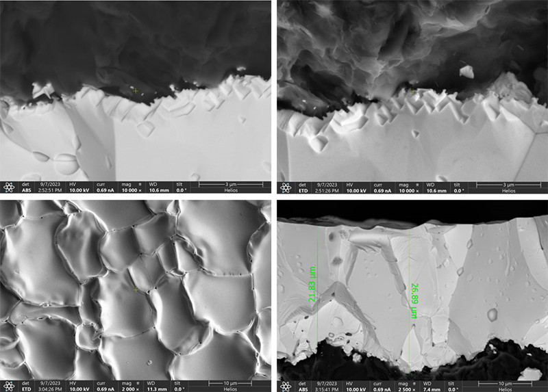
The TaC coating almost completely eliminates the carbon encapsulation phenomenon by isolating the direct contact between the graphite crucible and the SiC melt, significantly reducing the defect density of microtubes
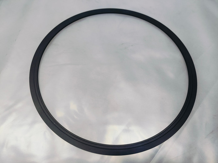
SiC ceramic is a ceramic material produced by the reaction of silicon (Si) and carbon (C) elements, featuring extremely high hardness, heat resistance and chemical stability
In the high-stakes world of semiconductor fabrication, precision and stability are everything—and that's where the Electrostatic Chuck (ESC) steps in. Far more than just a holding tool, the ESC uses electrostatic forces to securely clamp wafers during critical processes like etching, deposition, and ion implantation. But how does it actually work? Why is it superior to traditional mechanical clamping? And what role does it play in achieving nanoscale accuracy and throughput efficiency? Welcome to read.
The Dechuck principle of the Electrostatic Chuck is a key part of its workflow that involves electrostatic force elimination and wafer release mechanisms.
Glassy carbon is a non-graphitized carbon that combines the properties of glass and ceramics. It has many properties such as high temperature resistance, corrosion resistance, good electrical conductivity, etc. This blog analyzes the research history and future development trend of glassy carbon, which is worth reading.
We use cookies to offer you a better browsing experience, analyze site traffic and personalize content. By using this site, you agree to our use of cookies. Privacy Policy